Automatic Probe Station Measurement | Wafer Probe System Level Testing Equipment | SEMISHARE
SEMISHARE's fully automatic probe station measurement and wafer probe system level testing equipment can greatly boost testing efficiency and lower costs.
Advancing Semiconductor Testing: SEMISHARE's Cutting-Edge Probe Station Measurement Solutions
In the ever-evolving landscape of semiconductor manufacturing, the importance of precise and reliable testing cannot be overstated. As chips become smaller, more complex, and more powerful, the need for advanced probe station measurement and wafer level testing technologies has never been greater. SEMISHARE, a pioneer in semiconductor testing solutions, stands at the forefront of this technological revolution, offering state-of-the-art wafer probe systems and wafer test equipment that are reshaping the industry.
The Evolution of Wafer Probe Testing
Wafer probe testing has come a long way since its inception. Today, it's an integral part of the semiconductor manufacturing process, enabling manufacturers to identify and rectify issues before chips are packaged. But what exactly is a probe station for electrical measurements?
A probe station measurement system is a sophisticated piece of wafer test equipment designed to evaluate the electrical characteristics of semiconductor devices at the wafer level. It serves as the critical interface between the wafer and the test instruments, allowing for precise measurements and analysis. The probe station measurement setup typically includes a chuck to hold the wafer, microscopes for precise positioning, and manipulators to control the probe tips.
The importance of probe station measurement in the semiconductor industry cannot be overstated. It allows engineers to perform a wide range of tests, from basic continuity checks to complex RF measurements, all at the wafer level. This capability is crucial for ensuring the quality and reliability of semiconductor devices before they are packaged and sent to market.
The Importance of Wafer Level Testing
Wafer level testing, also known as wafer probe testing, is a crucial step in the semiconductor manufacturing process. It involves testing individual dies on a wafer before they are cut and packaged into separate chips. This approach offers several advantages:
1. Early defect detection: Identifying faulty dies before packaging saves time and resources.
2. Yield improvement: By pinpointing issues at the wafer level, manufacturers can optimize their processes for better yields.
3. Cost-effectiveness: Testing at the wafer level is more economical than testing packaged chips.
4. Performance characterization: Wafer level testing allows for detailed analysis of device performance under various conditions.
Wafer level testing is not just about identifying defective chips; it's a comprehensive process that provides valuable insights into the manufacturing process itself. By analyzing the data from wafer level testing, engineers can identify patterns and trends that can lead to process improvements and increased overall yield.
SEMISHARE's Wafer Probe System: A Closer Look
At the heart of SEMISHARE's offerings is its advanced wafer probe system. This system is designed to meet the demanding requirements of modern semiconductor testing, offering unparalleled precision, speed, and reliability.
Key features of SEMISHARE's wafer probe system include:
1. High-precision probing: Our system can accurately position probes on pads as small as 30 microns.
2. Multi-site testing: Test multiple dies simultaneously, significantly increasing throughput.
3. Temperature control: Test wafers across a wide temperature range, from -60°C to 300°C.
4. Automatic alignment: Advanced imaging systems ensure precise probe-to-pad alignment.
5. Flexible configuration: Easily adaptable to different wafer sizes and test requirements.
SEMISHARE's wafer probe system is not just a piece of equipment; it's a complete solution that integrates seamlessly with other wafer test equipment in the production line. The system's modular design allows for easy upgrades and customization, ensuring that it can adapt to changing testing requirements as semiconductor technology evolves.
Integrating Wafer Test Systems for Comprehensive Solutions
SEMISHARE's wafer probe system is designed to seamlessly integrate with our advanced wafer test systems, creating a comprehensive testing solution. Our wafer test systems are built to handle the most demanding semiconductor testing requirements, offering:
1. High-speed data acquisition and processing
2. Modular architecture for easy upgrades and customization
3. Support for a wide range of test parameters and conditions
4. Advanced software for test program development and data analysis
By combining our wafer probe system with our state-of-the-art wafer test systems, we provide a complete testing ecosystem that ensures accuracy, efficiency, and reliability throughout the testing process.
The Wafer Probing Process: From Start to Finish
Understanding the wafer probing process is crucial for appreciating the complexity and importance of this testing method. Here's a step-by-step breakdown:
1. Wafer loading: The wafer is carefully placed on the chuck of the probe station.
2. Alignment: The wafer is aligned with the probes using advanced imaging systems.
3. Probe contact: The probes make contact with the test pads on the wafer.
4. Test execution: Electrical tests are performed according to the predefined test program.
5. Data collection and analysis: Test results are gathered and analyzed in real-time.
6. Wafer mapping: A map of good and bad dies is generated based on the test results.
Each step in the wafer probing process is critical and requires precise control. SEMISHARE's wafer probe system ensures accuracy and repeatability at every stage, from initial wafer alignment to final data analysis.
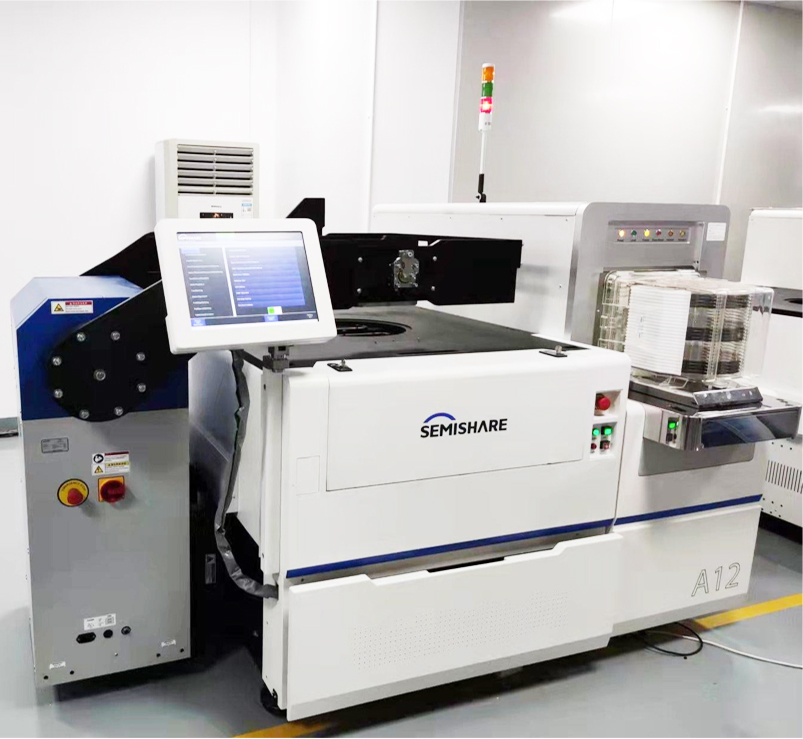
SEMISHARE's Automatic Probe Station: Revolutionizing Wafer Testing
In response to the growing demand for faster, more efficient testing, SEMISHARE has developed its automatic probe station. This advanced system takes wafer probe testing to the next level, offering:
1. Fully automated operation: From wafer loading to unloading, the entire process is automated.
2. High throughput: Test thousands of dies per hour with multi-site testing capabilities.
3. Exceptional accuracy: Advanced positioning systems ensure precise probe placement.
4. Flexible test programs: Easily customizable to meet specific testing requirements.
5. Real-time data analysis: Immediate feedback for process optimization.
SEMISHARE's automatic probe station is a game-changer in the world of wafer level testing. By automating the entire testing process, it not only increases throughput but also reduces the potential for human error, ensuring consistent and reliable results.
Advancing Automatic Prober Technology
In addition to our automatic probe station, SEMISHARE has made significant strides in automatic prober technology. Our automatic prober solutions are designed to maximize testing efficiency and accuracy, offering:
1. High-speed probe card alignment and contact
2. Advanced pattern recognition for precise die targeting
3. Intelligent probe tip cleaning and maintenance systems
4. Compatibility with a wide range of probe card types
Our automatic prober technology works in tandem with our wafer test systems to provide a seamless, high-throughput testing solution. This integration allows for rapid, accurate testing of even the most complex semiconductor devices.
The Evolution of Automatic Prober Technology
SEMISHARE's commitment to innovation is evident in our continuous improvement of automatic prober technology. Our latest models, including the advanced aotomatic prober, represent the pinnacle of wafer testing automation, offering:
1. Enhanced throughput: Our aotomatic prober can test more dies per hour than ever before, significantly increasing production efficiency.
2. Improved accuracy: Advanced positioning systems and calibration techniques ensure precise probe placement, even on the smallest of contact pads.
3. Greater flexibility: Our aotomatic prober is designed to handle a wide range of wafer sizes and types, from standard silicon wafers to advanced compound semiconductors.
4. Intelligent self-diagnostics: Built-in monitoring systems continuously check the aotomatic prober's performance, alerting operators to potential issues before they impact testing quality.
5. Seamless integration: Our aotomatic prober is designed to work seamlessly with our wafer test systems and other semiconductor manufacturing equipment, creating a cohesive testing ecosystem.
By leveraging these advanced aotomatic prober capabilities, semiconductor manufacturers can significantly streamline their testing processes, reduce human error, and improve overall product quality. The aotomatic prober has become an indispensable tool in modern semiconductor manufacturing, enabling the high-volume production of increasingly complex and miniaturized devices.
As we look to the future, SEMISHARE continues to invest in aotomatic prober research and development, ensuring that our customers always have access to the most advanced and efficient testing technologies available.
The Future of Wafer Test Systems
As semiconductor technology continues to advance, so too must the wafer test systems used to evaluate them. SEMISHARE is committed to staying ahead of the curve, continuously innovating to meet the evolving needs of the industry.
Some of the trends we're exploring for future wafer test systems include:
1. AI-driven testing: Using artificial intelligence to optimize test programs and predict potential issues.
2. Advanced materials: Developing new probe materials for improved performance and longevity.
3. Enhanced parallelism: Testing even more dies simultaneously for increased throughput.
4. Improved thermal management: Better temperature control for more accurate testing across wider temperature ranges.
These advancements in wafer test systems will enable semiconductor manufacturers to keep pace with the rapid evolution of chip technology, ensuring that they can continue to produce high-quality, reliable devices even as complexity increases and feature sizes shrink.
SEMISHARE's Commitment to Innovation
At SEMISHARE, we understand that the future of semiconductor manufacturing depends on continuous innovation in testing methodologies. Our commitment to advancing probe station measurement and wafer level testing capabilities is evident in our ongoing research and development efforts.
Our High-Performance™ Technology, for instance, provides a highly stable fully automatic wafer probe table and test equipment. This patented technology addresses the challenge of equipment vibration during testing, ensuring consistent and accurate results.
SEMISHARE's innovation extends beyond hardware. We also develop advanced software solutions that work in tandem with our wafer probe systems and wafer test equipment to provide comprehensive testing capabilities. Our software suite includes features such as:
1. Intuitive test program development tools
2. Advanced data analysis and visualization capabilities
3. Integration with factory automation systems
4. Customizable reporting tools
This combination of cutting-edge hardware and sophisticated software makes SEMISHARE's wafer test systems some of the most advanced and user-friendly in the industry.
The Role of Wafer Test Equipment in Quality Assurance
Wafer test equipment plays a crucial role in ensuring the quality and reliability of semiconductor devices. By performing comprehensive tests at the wafer level, manufacturers can:
1. Identify and eliminate defective dies before packaging
2. Characterize device performance under various conditions
3. Ensure consistency across large production runs
4. Provide valuable data for process improvement
SEMISHARE's wafer test equipment is designed to meet these challenges head-on. Our systems provide the accuracy, speed, and flexibility needed to perform a wide range of tests, from basic parametric measurements to complex functional tests.
Advancing Wafer Probe Testing for Next-Generation Devices
As semiconductor devices continue to evolve, so too must the methods used to test them. SEMISHARE is at the forefront of developing advanced wafer probe testing techniques for next-generation devices, including:
1. 3D integrated circuits
2. Advanced packaging technologies
3. High-frequency RF devices
4. Power semiconductors
Our wafer probe testing solutions are designed to handle the unique challenges posed by these advanced devices, ensuring that manufacturers can maintain high quality standards even as technology pushes the boundaries of what's possible.
The Importance of Wafer Level Reliability Testing
Wafer level reliability testing is becoming increasingly important as semiconductor devices are used in more critical applications. This type of testing involves subjecting devices to stress conditions at the wafer level to predict their long-term reliability.
SEMISHARE's wafer test systems include features specifically designed for wafer level reliability testing, such as:
1. Precise temperature control for accelerated life testing
2. Ability to apply high voltages and currents for stress testing
3. Long-term test capabilities for burn-in testing at the wafer level
4. Advanced data analysis tools for reliability prediction
By performing reliability testing at the wafer level, manufacturers can identify potential reliability issues early in the production process, saving time and resources while ensuring the highest levels of product quality.
The Synergy of Automatic Probe Stations and Wafer Test Systems
At SEMISHARE, we understand that the key to efficient semiconductor testing lies in the seamless integration of automatic probe stations and wafer test systems. Our automatic probe stations, including the advanced aotomatic prober, are designed to work in perfect harmony with our wafer test systems, creating a unified testing environment that maximizes productivity and accuracy.
The advantages of this integrated approach include:
1. Streamlined workflow: Our aotomatic prober and wafer test systems share a common interface, reducing training time and minimizing errors.
2. Enhanced data management: Test results from the aotomatic prober are seamlessly transferred to the wafer test system for comprehensive analysis.
3. Improved throughput: The coordination between the aotomatic prober and wafer test system minimizes downtime and maximizes testing efficiency.
4. Flexible configuration: Our systems can be easily customized to meet specific testing requirements, ensuring that you have the right tools for your unique needs.
By leveraging the power of our aotomatic prober in conjunction with our advanced wafer test systems, semiconductor manufacturers can achieve unprecedented levels of testing accuracy and efficiency.
Conclusion: Empowering the Future of Semiconductor Manufacturing
As the semiconductor industry continues to push the boundaries of what's possible, the role of advanced wafer probe testing and wafer level testing becomes increasingly critical. SEMISHARE's comprehensive suite of probe station measurement, wafer probe system, wafer test equipment, and aotomatic prober technologies empowers semiconductor manufacturers to:
1. Accelerate time-to-market for new devices
2. Improve yield rates through early defect detection
3. Enhance device performance through precise characterization
4. Reduce overall testing costs through efficient and accurate methodologies
By partnering with SEMISHARE, semiconductor companies gain access to cutting-edge testing solutions that drive innovation and ensure the highest standards of quality and reliability. Our commitment to advancing wafer probe testing and wafer level testing methodologies positions us as a key enabler in the ongoing evolution of semiconductor technology.
The future of semiconductor manufacturing is bright, and SEMISHARE is proud to be at the forefront of this exciting industry. Our continued investment in research and development ensures that we will remain a leader in semiconductor testing technology for years to come.
As we continue to innovate in the field of semiconductor testing, SEMISHARE remains committed to developing cutting-edge wafer test systems, aotomatic probers, and automatic probe stations. These technologies, working in concert, provide the foundation for the next generation of semiconductor manufacturing and testing.
Whether you're developing cutting-edge processors, high-performance memory devices, or advanced sensors, SEMISHARE has the wafer test systems and wafer probe testing solutions you need to ensure the quality and reliability of your products. Our commitment to innovation ensures that our wafer test systems and aotomatic probers will continue to meet the challenges of tomorrow's semiconductor technologies.
For more information on how SEMISHARE's advanced semiconductor test solutions can empower your research or production processes, visit our website at https://www.semishareprober.com/. Discover how our expertise in probe station measurement, wafer level testing, and wafer probe systems can help you achieve new heights in semiconductor innovation and manufacturing excellence.
Join us in shaping the future of semiconductor technology. With SEMISHARE as your testing partner, you'll be well-equipped to meet the challenges of today's semiconductor industry and ready to seize the opportunities of tomorrow.