
Test Solution
Silicon photonic devices, based on the optoelectronic conversion effect, are widely used in optical communications, optical sensing, optical computing, and other fields. Their core components include optical chips, optical modules, and complex optoelectronic devices (such as laser diodes, photodetectors, etc.). Due to the high integration density, multi-channel interaction, and precise alignment requirements of silicon photonic components, testing must cover multi-dimensional characteristics—including physical, optical, and electrical properties—to ensure performance and reliability.
High-Precision Coupling Requirements: Silicon photonic components present significant coupling challenges with time-consuming processes, requiring solutions for low coupling efficiency and high insertion loss.
Multi-Degree-of-Freedom Alignment: Multi-channel I/O interfaces demand simultaneous optimization across multiple alignment degrees of freedom (e.g., positional, angular) for precise optical path matching.
Automated Testing: Traditional testing methods rely too much on manual work, struggling to meet parallel testing demands for highly complex photonic integrated circuits (PICs).
Throughput-Precision Tradeoff: Sub-micron alignment accuracy must be maintained under high-speed testing conditions—particularly critical for Micro-LEDs and other precision-sensitive devices.
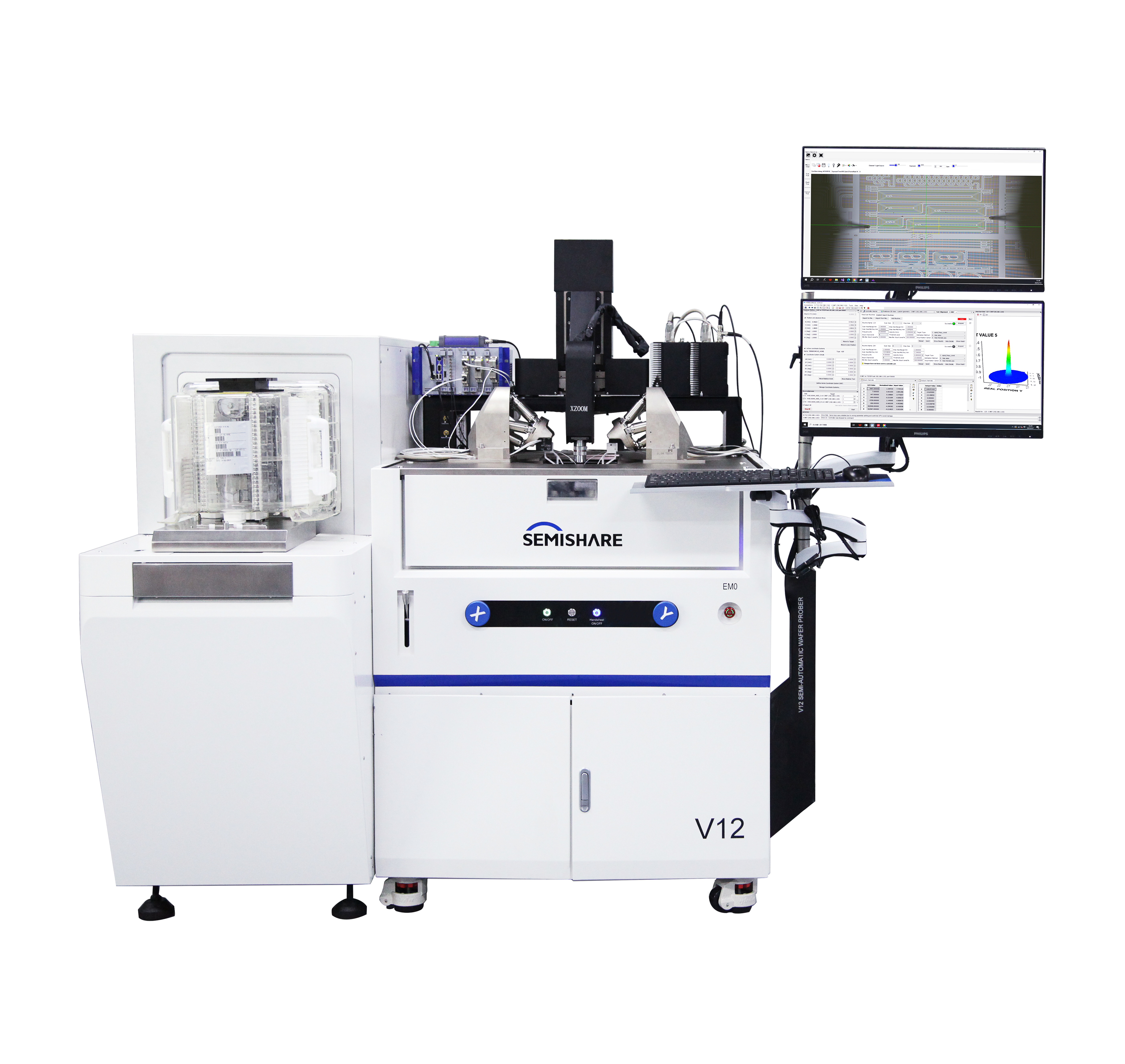
Based on the SEMISHARE V-series semi-automatic probe station, integrated with PI’s six-axis high-precision fiber alignment system, this is an efficient semi-automatic probe station testing system specifically designed for silicon photonic device testing.
Silicon photonic testing faces significant challenges in achieving correct coupling, which is both highly difficult and time-consuming. Furthermore, today’s silicon photonic components are more complex than ever, featuring multiple interacting inputs/outputs, multi-channel configurations, and component alignment—all of which require optimization across multiple degrees of freedom (DOF) to ensure accurate testing.
SEMISHARE’s integrated PI alignment automation solution, powered by a deep toolkit of firmware algorithms, delivers precise optimization. Its unique fully parallel technology enables optimization across multiple DOFs, multiple inputs/outputs spanning different channels, and even simultaneous optimization for multiple devices.
The SEMISHARE V-series silicon photonic testing system integrates PI’s six-axis high-precision fiber alignment system. This six-axis stage-based solution offers a freely selectable pivot point, allowing users to optimize alignment by rotating around the beam waist, focal point, or optical axis—further enhancing testing efficiency.
>V Series New Generation High Performance Probe StationLearn More
Silicon photonic devices
1.The industry's fastest test system, with travel speeds exceeding 70mm/s and sub-micron motion accuracy.
2. XY-axis repeatability: ±1µm, Z-axis repeatability: ±1µm.
3. Wide temperature range (-50°C to 200°C) with exceptional chuck flatness under extreme thermal conditions.
4. Temperature control accuracy & stability: better than 0.1°C.
5. Triaxial (Signal, Guard, Ground) structure, enabling fA-level electrical testing and ultra-low parasitic capacitance.
6. Femto-Guard™ design for minimal system leakage current.
7. EMI & spectral noise shielding (light-sealed chamber) for optimal low-noise testing environment.
1.Move to calibration position
2.Single fiber/FA position measurement
3.Adjust θz (W)\0x (U)\y (V)
4.Single fiber/FA extension length measurement
5.Move to test-ready position
6.Move to coupling position
7.Search for initial light signal
8.Fast coupling alignment
9.Silicon photonic parameter measurement
1.The automatic coupling of fiber probes is achieved using a 6-axis displacement stage, with an additional piezoelectric ceramic nano-positioner for high-precision, highly repeatable sub-micron alignment.
2. Optical component testing and packaging face multi-degree-of-freedom challenges. The system enables high-speed alignment through built-in subroutines, utilizing detection, area scanning, and gradient scanning algorithms suitable for various coupling processes. It achieves fast, reliable alignment within 1 second and supports automated scan data modeling to precisely locate optimal values even during rapid coarse scans.
3. Modular and flexible configurations are supported, including loader integration for fully automated testing. The system ensures seamless transition from lab (LAB) to production line (FAB), meeting standardized testing requirements for OSAT/Foundries and optical modules/engines.
4. A multi-magnification optical display system provides high-precision measurement and dynamic monitoring.
5. The system supports wafer-level (8″–12″), multi-chip, and single-chip testing, with reserved interfaces for RF and electrical testing modules, accommodating full optoelectronic testing needs (OO/OE/EO/RF).
 Request for quotation

0755-2690 6952 turn 801/804/806/814
 Send Email
