Semiconductor Testing in Vacuum Environment | SEMISHARE
SEMISHARE's innovative semiconductor testing solutions, featuring our patented SpecialConditions technology, delivering high stability in vacuum test environment.
Semiconductor Testing: Advancing Precision and Reliability with SEMISHARE Prober
In the ever-evolving landscape of semiconductor technology, the importance of rigorous and comprehensive testing cannot be overstated. SEMISHARE Prober, a pioneer in semiconductor test equipment and methodologies, is at the forefront of this critical industry, providing cutting-edge solutions that ensure the quality, reliability, and performance of semiconductor devices. This article delves into the intricacies of semiconductor testing, exploring its significance, methodologies, and the innovative approaches developed by SEMISHARE Prober.
Understanding Semiconductor Testing
What is a semiconductor test? At its core, a semiconductor test is a multifaceted process designed to evaluate the electrical characteristics, functionality, and reliability of semiconductor devices. This comprehensive assessment is crucial in verifying that these devices meet the stringent specifications required for their intended applications. SEMISHARE Prober's advanced semiconductor testing solutions encompass a wide range of tests, from basic parametric measurements to complex functional evaluations under extreme environmental conditions.
The importance of semiconductor testing cannot be overstated. As semiconductor devices become increasingly complex and are integrated into critical systems across various industries, the need for thorough and accurate testing grows exponentially. Semiconductor testing is vital for several reasons:
1. Quality Assurance: It ensures that each device meets the required performance standards.
2. Reliability: Testing helps predict the long-term reliability of devices under various operating conditions.
3. Yield Improvement: By identifying defects early in the manufacturing process, testing helps improve overall production yield.
4. Cost Reduction: Early detection of issues reduces the cost associated with failures in later stages of production or in the field.
5. Innovation Support: Comprehensive testing enables engineers to push the boundaries of semiconductor technology, supporting the development of more advanced devices.
Types of Semiconductor Tests
Semiconductor testing encompasses various types of assessments, each designed to evaluate specific aspects of a device's performance. One crucial type is the function test for a semiconductor. This test verifies that the semiconductor device performs its intended operations correctly. Function tests can range from simple logic checks in digital circuits to complex signal processing evaluations in analog devices.
Other types of semiconductor tests include:
1. Parametric Tests: Measure basic electrical parameters such as voltage, current, and resistance.
2. AC Tests: Evaluate the device's performance with alternating current signals.
3. RF Tests: Assess the high-frequency characteristics of devices used in wireless communications.
4. Power Tests: Examine the device's behavior under various power conditions.
5. Reliability Tests: Subject devices to stress conditions to predict long-term performance.
SEMISHARE Prober's semiconductor testing technology addresses all these aspects, providing a comprehensive suite of testing solutions that cater to the diverse needs of the semiconductor industry.
How Are Semiconductors Inspected?
The inspection of semiconductors is a critical part of the testing process. It involves both visual and electrical examinations to detect any physical defects or electrical abnormalities. SEMISHARE Prober employs advanced inspection techniques that include:
1. Automated Optical Inspection (AOI): High-resolution cameras and image processing algorithms detect visual defects.
2. Electron Microscopy: For nanoscale inspection of semiconductor structures.
3. X-ray Inspection: To examine internal structures and connections in packaged devices.
4. Electrical Probing: Using precision probes to test electrical characteristics at various points on the wafer.
These inspection methods are integrated into SEMISHARE Prober's semiconductor testing systems, ensuring a thorough evaluation of each device.
Measuring Semiconductors: Precision and Accuracy
How do you measure a semiconductor? This question is central to the semiconductor testing process. Measuring a semiconductor involves assessing various electrical properties with extreme precision. SEMISHARE Prober's advanced measurement techniques include:
1. I-V Characterization: Measuring current-voltage relationships to determine device behavior.
2. C-V Analysis: Evaluating capacitance-voltage characteristics for device profiling.
3. High-Frequency Measurements: Assessing performance at radio and microwave frequencies.
4. Thermal Characterization: Measuring device performance across a range of temperatures.
SEMISHARE Prober's semiconductor test equipment is designed to provide highly accurate measurements, often at the picosecond and femtoamp levels, ensuring the utmost precision in device characterization.
SEMISHARE Prober's Innovative Approach to Semiconductor Testing
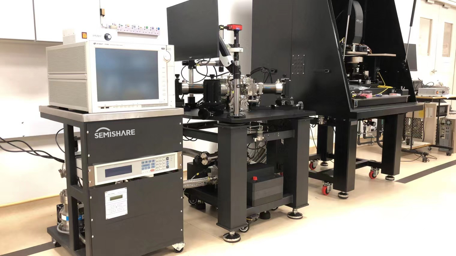
SEMISHARE Prober's approach to semiconductor testing is characterized by innovation and a deep understanding of industry needs. The company's SpecialConditionsTM technology exemplifies this approach. This patented technology provides a semiconductor device test probe station and method capable of creating integrated high-temperature and low-temperature vacuum test environments.
Key features of SpecialConditionsTM technology include:
1. Vacuum Chamber: Simulates space-like conditions for testing aerospace-grade semiconductors.
2. Temperature Control: Enables testing from cryogenic to high temperatures.
3. Radiation Shielding: Protects sensitive measurements from external interference.
4. Magnetic Field Generation: For testing devices under various magnetic conditions.
5. Particle Irradiation Capability: Simulates the effects of cosmic radiation on semiconductor devices.
This technology is particularly crucial for testing high-reliability semiconductor devices intended for aerospace applications, where the operating environment is extremely harsh and unforgiving.
Application in Research and Industry
SEMISHARE Prober's semiconductor testing solutions find applications in both research institutions and industrial settings. The deployment of the SEMISHARE CG-C-2 Probe Station at the National University of Singapore demonstrates the technology's capability in advanced research environments. In industry, SEMISHARE Prober's solutions are used for:
1. Wafer-level Testing: Evaluating devices before they are cut from the wafer.
2. Package-level Testing: Assessing the performance of packaged semiconductor devices.
3. Reliability Testing: Conducting long-term stress tests to predict device lifespan.
4. Failure Analysis: Identifying the root causes of device failures.
Complementary Technologies
SEMISHARE Prober's semiconductor testing capabilities are enhanced by complementary technologies:
1. Air-Floating Chuck Moving Technology: Enables precise and smooth wafer movement during testing.
2. Semi-Automatic Probe Station Measurement Technology: Balances automation with manual control for flexible testing scenarios.
3. Fully Automatic Probe Station Measurement Technology: Provides high-throughput testing for production environments.
These technologies work in concert to provide a comprehensive semiconductor testing solution that addresses the diverse needs of the industry.
The Future of Semiconductor Testing
As semiconductor technology continues to advance, so too must the testing methodologies and equipment. SEMISHARE Prober is committed to staying at the forefront of these advancements. Future developments in semiconductor testing are likely to include:
1. Increased Integration of AI and Machine Learning: For more intelligent and adaptive testing processes.
2. Enhanced 3D Testing Capabilities: As 3D chip structures become more prevalent.
3. Faster and More Precise Measurements: To keep pace with increasing device speeds and smaller feature sizes.
4. Greater Emphasis on Reliability Testing: As semiconductors are deployed in more critical applications.
5. Expanded Environmental Testing: To simulate a wider range of operating conditions.
SEMISHARE Prober is actively researching and developing solutions to meet these future challenges, ensuring that its semiconductor testing technology remains at the cutting edge.
Semiconductor testing is a critical process in the production of reliable and high-performance electronic devices. SEMISHARE Prober's advanced semiconductor testing technology plays a vital role in ensuring the quality and reliability of semiconductor devices across various applications, from consumer electronics to aerospace systems.
By providing comprehensive solutions for semiconductor testing, from function tests to specialized environmental simulations, SEMISHARE Prober enables manufacturers and researchers to push the boundaries of semiconductor technology. As the industry continues to evolve, SEMISHARE Prober remains committed to innovation, developing new testing methodologies and equipment that will meet the challenges of tomorrow's semiconductor devices.
For more information on how SEMISHARE Prober's semiconductor testing solutions can enhance your manufacturing or research capabilities, visit https://www.semishareprober.com/. Discover how our advanced technology can help you achieve new levels of precision, reliability, and efficiency in semiconductor testing.