Semiconductor Wafer Prober Testing | RF Test Probes | SEMISHARE
SEMISHARE's cutting-edge semiconductor wafer prober testing solutions and RF test probes are transforming on-wafer testing. Learn about our latest advancements.
SEMISHARE: Pioneering Advanced Semiconductor Testing Solutions
In the rapidly evolving landscape of semiconductor technology, the importance of precise and reliable testing cannot be overstated. As the industry pushes the boundaries of performance and miniaturization, the need for advanced probe test solutions and sophisticated on wafer testing methodologies has become more critical than ever. SEMISHARE, a leading innovator in semiconductor test equipment, stands at the forefront of this technological revolution, offering cutting-edge test probes, rf test probes, and comprehensive semiconductor test probes that are reshaping the landscape of wafer testing.
Understanding the Fundamentals of Probe Testing
Probe test technology is at the heart of semiconductor manufacturing and validation processes. A test probe serves as the critical interface between test equipment and the device under test (DUT), allowing for precise measurement of electrical characteristics and performance parameters. SEMISHARE's advanced test probe solutions are designed to meet the exacting demands of modern semiconductor testing, offering unparalleled accuracy, reliability, and versatility across a wide range of applications.
How does a test probe work?
A test probe establishes a secure electrical connection with the DUT, typically through direct contact with test pads or bumps on the wafer surface. The probe transmits electrical signals to the device and measures the resulting responses, enabling engineers to evaluate various aspects of the semiconductor's performance, including voltage, current, resistance, and frequency response.
Types of Test Probes
SEMISHARE offers a comprehensive range of test probes to address diverse testing requirements:
1. DC Probes: Used for measuring static electrical properties and low-frequency signals.
2. AC Probes: Designed for testing alternating current characteristics and dynamic behavior.
3. RF Test Probes: Specialized probes for high-frequency and radio frequency measurements.
4. Semiconductor Test Probes: Custom-designed probes for specific semiconductor device testing requirements.
Accepted Methods for Probe Testing
The semiconductor industry relies on several established probe test methodologies:
1. DC Parametric Testing: Measuring static electrical properties such as resistance, voltage thresholds, and leakage currents.
2. AC Characterization: Evaluating dynamic behavior and frequency response of devices.
3. RF Performance Testing: Assessing high-frequency characteristics crucial for wireless and communication applications.
4. Functional Testing: Verifying the overall functionality and performance of the device under various operating conditions.
Advancing RF Wafer Probe Technology
As the demand for high-frequency devices continues to grow, the importance of advanced rf wafer probe technology cannot be overstated. SEMISHARE has been at the forefront of developing cutting-edge rf wafer probe solutions that address the unique challenges posed by radio frequency testing on semiconductor wafers.
Our rf wafer probe systems are designed to provide accurate and reliable measurements across a wide range of frequencies, from sub-GHz to mmWave. The precision-engineered probe tips ensure optimal contact with the device under test, minimizing parasitic effects and maintaining signal integrity throughout the measurement process.
Key features of SEMISHARE's rf wafer probe technology include:
1. Wide bandwidth capability: Our rf wafer probe solutions support measurements up to 120 GHz and beyond, making them ideal for next-generation wireless and 5G applications.
2. Low insertion loss: Advanced materials and design techniques minimize signal attenuation, ensuring accurate measurements even at the highest frequencies.
3. Customizable probe configurations: We offer a range of rf wafer probe options to accommodate various device layouts and pad geometries.
4. Integration with automated test systems: Our rf wafer probe solutions can be seamlessly integrated with automated wafer probers for high-volume testing.
5. Temperature-controlled testing: Many of our rf wafer probe systems include options for heated or cooled chucks, enabling device characterization across a wide temperature range.
The use of advanced rf wafer probe technology is critical in the development and production of high-frequency semiconductor devices. By providing accurate on-wafer measurements, SEMISHARE's rf wafer probe solutions help engineers optimize device performance, reduce design cycles, and improve overall product quality.
Enhancing Semiconductor Test Probes for Next-Generation Devices
As semiconductor devices continue to shrink in size and increase in complexity, the demands placed on semiconductor test probes have grown exponentially. SEMISHARE's advanced semiconductor test probes are designed to meet these challenges head-on, offering unparalleled precision and reliability in wafer-level testing.
Our semiconductor test probes are engineered to address the specific needs of various device types, including:
1. Logic and memory devices
2. Analog and mixed-signal ICs
3. RF and microwave components
4. Power semiconductors
5. MEMS and sensors
Key innovations in SEMISHARE's semiconductor test probes include:
1. Ultra-fine pitch capability: Our advanced probe technologies can accommodate pad pitches down to 30 microns and below, enabling testing of the most densely packed chips.
2. Multi-DUT testing: Many of our semiconductor test probes are designed for parallel testing of multiple devices, significantly increasing throughput and reducing overall test time.
3. High-frequency performance: Specialized semiconductor test probes for RF and microwave applications maintain signal integrity up to mmWave frequencies.
4. Robust design: Our semiconductor test probes are built to withstand millions of touchdowns, ensuring long-term reliability and reduced maintenance costs.
5. Customizable tip geometries: We offer a wide range of probe tip shapes and materials to optimize contact resistance and minimize pad damage.
By continually advancing our semiconductor test probe technology, SEMISHARE enables our customers to stay ahead of the curve in semiconductor testing, ensuring that they can accurately characterize and validate even the most advanced devices.
Revolutionizing On Wafer Testing Methodologies
On wafer testing has become an indispensable part of the semiconductor manufacturing process, allowing for early detection of defects and comprehensive device characterization before packaging. SEMISHARE's advanced on wafer testing solutions are designed to maximize efficiency, accuracy, and flexibility in this critical phase of production.
Our on wafer testing systems incorporate several key technologies:
1. High-precision probe positioning: Automated systems ensure accurate and repeatable probe placement across the wafer, with positioning resolution down to sub-micron levels.
2. Advanced chuck technologies: Temperature-controlled chucks enable device testing across a wide range of operating conditions, from cryogenic temperatures to over 300°C.
3. Integrated measurement capabilities: Our on wafer testing solutions seamlessly interface with a variety of test and measurement equipment, including network analyzers, parametric testers, and high-speed digital test systems.
4. Automated pattern recognition: Advanced imaging and pattern recognition algorithms facilitate rapid die identification and probe alignment, reducing overall test time.
5. Flexible probe card compatibility: Our on wafer testing systems support a wide range of probe card technologies, including vertical, cantilever, and MEMS-based designs.
SEMISHARE's commitment to advancing on wafer testing methodologies extends beyond hardware innovations. We also provide comprehensive software solutions that streamline test program development, data analysis, and results reporting. This integrated approach to on wafer testing helps our customers:
1. Reduce time-to-market for new semiconductor products
2. Improve overall yield through early defect detection
3. Optimize device performance through comprehensive characterization
4. Lower testing costs through increased efficiency and automation
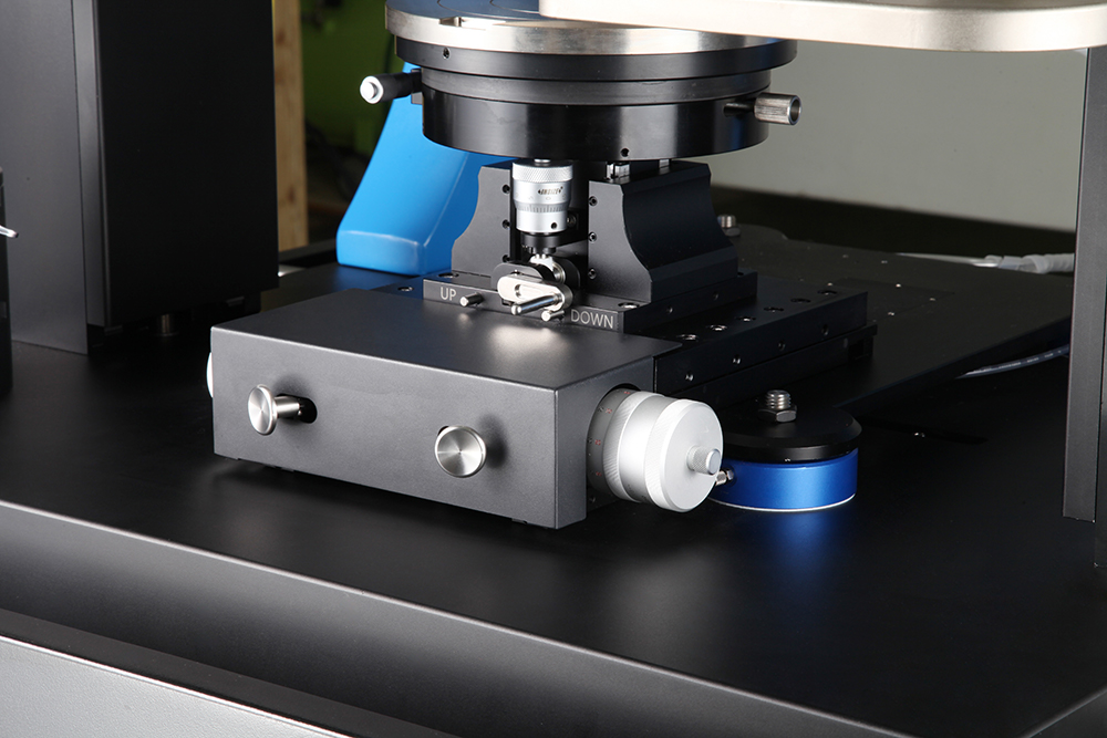
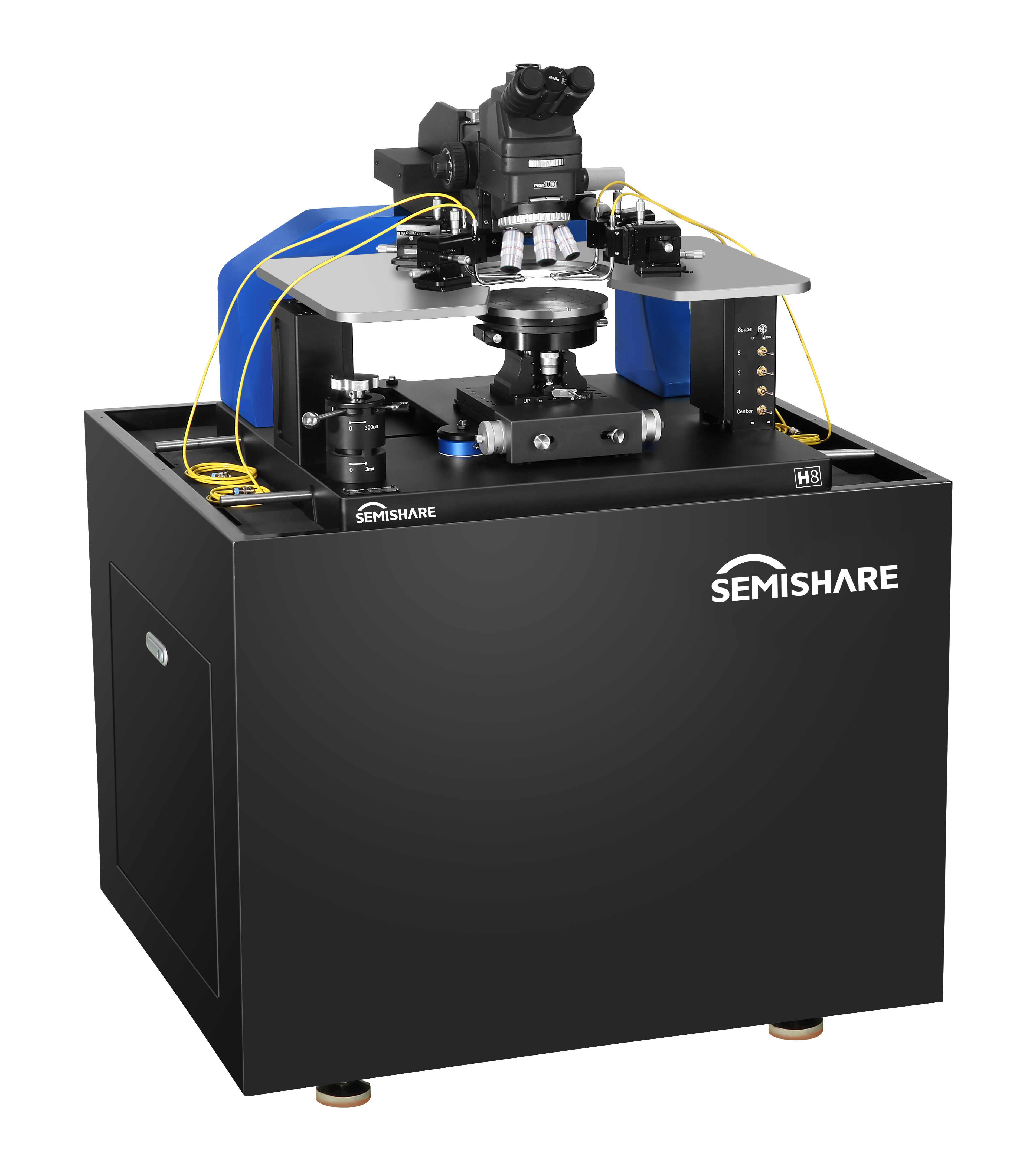
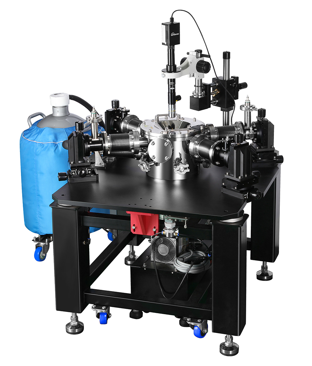
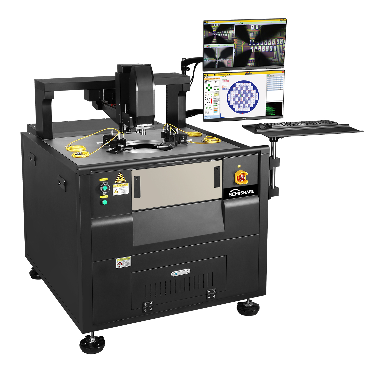
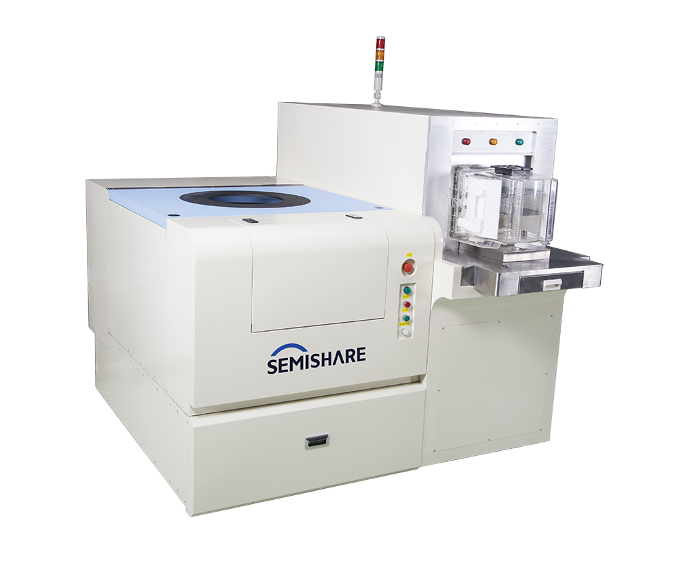
Semiconductor Wafer Prober: The Foundation of Efficient Testing
At the heart of any advanced wafer testing setup lies the semiconductor wafer prober. SEMISHARE's state-of-the-art semiconductor wafer prober systems represent the culmination of years of research and development in precision mechanics, automation, and test integration.
Our semiconductor wafer prober solutions offer:
1. High-speed wafer handling: Automated wafer loading and unloading systems minimize handling time and reduce the risk of wafer damage.
2. Precision stage control: Advanced motion control systems provide sub-micron positioning accuracy, ensuring precise probe placement even on the smallest pad sizes.
3. Flexible chuck options: We offer a range of chuck technologies to suit various testing needs, including thermal chucks for temperature-dependent measurements and vacuum chucks for secure wafer holding.
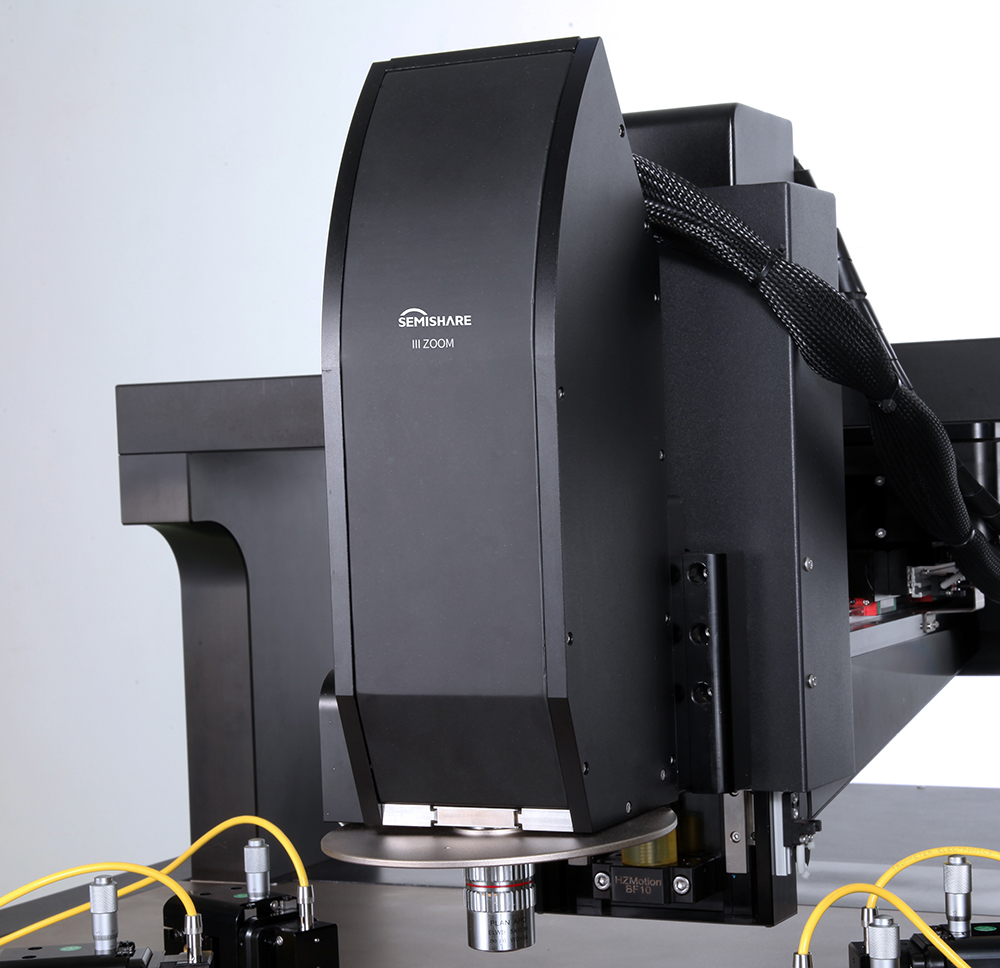
4. Integrated vision systems: High-resolution cameras and advanced image processing algorithms facilitate rapid wafer alignment and probe positioning.
5. Modular design: Our semiconductor wafer prober systems can be easily configured and upgraded to accommodate changing test requirements and new device technologies.
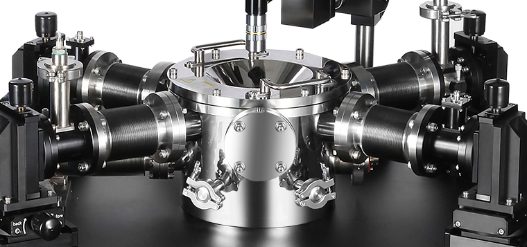
6. Environmental control: Many of our semiconductor wafer prober models include options for EMI shielding and vibration isolation, ensuring optimal measurement conditions.
7. Seamless software integration: SEMISHARE's prober control software interfaces with a wide range of test equipment and automation platforms, enabling smooth integration into existing test workflows.
The Role of Semiconductor Wafer Probers in Advanced Packaging
As advanced packaging technologies like 2.5D and 3D IC become more prevalent, the role of the semiconductor wafer prober in testing these complex structures has expanded. SEMISHARE's advanced semiconductor wafer prober systems are designed to address the unique challenges posed by these new packaging paradigms, including:
1. Testing of high-density interposers
2. Probing of through-silicon vias (TSVs)
3. Known-good-die (KGD) testing for stacked die applications
4. Fine-pitch micro-bump probing for flip-chip devices
By continually innovating our semiconductor wafer prober technology, SEMISHARE ensures that our customers are well-equipped to handle the testing challenges of both current and future semiconductor devices.
Advancing Probe Test Methodologies
At SEMISHARE, we continuously strive to enhance our probe test capabilities to meet the evolving needs of the semiconductor industry. Our advanced probe test solutions are designed to address the challenges of testing increasingly complex and miniaturized devices. By leveraging cutting-edge technologies and innovative approaches, we've developed probe test systems that offer unparalleled accuracy, speed, and reliability.
One of the key areas where our probe test technology shines is in the testing of high-speed digital circuits. Our probe test solutions incorporate advanced signal integrity techniques to ensure accurate measurements even at the highest data rates. This capability is crucial for validating the performance of next-generation communication chips and high-speed memory devices.
Moreover, our probe test systems are equipped with intelligent automation features that streamline the testing process and reduce the potential for human error. These automated probe test routines can significantly increase throughput while maintaining the highest standards of measurement accuracy.
SEMISHARE's probe test solutions also excel in the realm of power semiconductor testing. Our specialized probe test setups can handle high voltages and currents, allowing for comprehensive characterization of power devices such as IGBTs, MOSFETs, and wide-bandgap semiconductors like SiC and GaN.
Innovations in RF Test Probes
The field of RF testing is experiencing rapid growth, driven by the proliferation of wireless technologies and the advent of 5G networks. To meet these challenges, SEMISHARE has made significant investments in developing state-of-the-art rf test probes.
Our latest generation of rf test probes incorporates advanced materials and precision manufacturing techniques to achieve superior high-frequency performance. These rf test probes maintain excellent signal integrity up to mmWave frequencies, making them ideal for testing cutting-edge 5G and beyond-5G devices.
SEMISHARE's rf test probes are designed with versatility in mind. They can be easily integrated into various test setups, from manual probe stations to fully automated wafer-level test systems. This flexibility allows our customers to leverage the same high-performance rf test probes across different stages of their product development and manufacturing processes.
To complement our rf test probes, we've also developed a suite of calibration and de-embedding tools. These software solutions help engineers extract accurate device characteristics from raw measurement data, accounting for the effects of the rf test probes and associated fixtures.
Furthermore, our rf test probes are compatible with a wide range of RF and microwave measurement equipment, including vector network analyzers, spectrum analyzers, and signal generators. This broad compatibility ensures that our rf test probes can seamlessly integrate into existing test environments, maximizing the value of our customers' equipment investments.
In response to the growing demand for over-the-air (OTA) testing of 5G devices, SEMISHARE has also introduced specialized rf test probes designed for near-field probing of antennas and antenna arrays. These rf test probes enable detailed characterization of antenna radiation patterns and help optimize the performance of complex multi-antenna systems.
By continually pushing the boundaries of rf test probe technology, SEMISHARE ensures that our customers have the tools they need to stay competitive in the rapidly evolving world of RF and wireless communications.
SEMISHARE's Commitment to Innovation in Wafer Testing
At SEMISHARE, we understand that the future of semiconductor technology relies on continuous innovation in testing methodologies. Our commitment to advancing wafer testing capabilities is evident in our ongoing research and development efforts:
1. Advanced Materials: Developing probe tips with novel materials for enhanced durability and electrical performance.
2. Intelligent Testing Algorithms: Implementing AI-driven test optimization to reduce test times and improve coverage.
3. Integrated Measurement Solutions: Creating seamless interfaces between probe systems and advanced measurement equipment.
The SEMISHARE Advantage in Semiconductor Testing
Choosing SEMISHARE as your partner in semiconductor testing offers numerous advantages:
1. Comprehensive Solutions: From individual test probes to fully integrated wafer testing systems, SEMISHARE provides end-to-end solutions for semiconductor characterization.
2. Customization Capabilities: Our team of experts works closely with clients to develop tailored testing solutions for unique device requirements.
3. Global Support Network: With a worldwide presence, SEMISHARE offers local support and rapid response times to meet your testing needs.
4. Continuous Innovation: Our commitment to research and development ensures that our clients always have access to the latest advancements in probe test technology.
Conclusion: Empowering the Future of Semiconductor Innovation
As the semiconductor industry continues to evolve, the importance of advanced test solutions cannot be overstated. SEMISHARE's comprehensive suite of rf wafer probe, semiconductor test probes, on wafer testing, and semiconductor wafer prober technologies empowers our customers to stay at the forefront of semiconductor innovation.
Our commitment to ongoing research and development ensures that we continue to push the boundaries of what's possible in semiconductor testing. By partnering with SEMISHARE, semiconductor manufacturers and researchers gain access to:
1. Cutting-edge rf wafer probe solutions for high-frequency device characterization
2. Advanced semiconductor test probes capable of testing the most complex and densely packed chips
3. Comprehensive on wafer testing methodologies that improve yield and reduce time-to-market
4. State-of-the-art semiconductor wafer prober systems that form the foundation of efficient and accurate testing
As we look to the future, SEMISHARE remains dedicated to advancing the field of semiconductor test technology. Our ongoing investments in areas such as artificial intelligence, machine learning, and advanced materials promise to unlock new possibilities in device characterization and testing efficiency.
For more information on how SEMISHARE's advanced semiconductor test solutions can empower your research or production processes, visit our website at https://www.semishareprober.com/. Discover how our expertise in rf wafer probe technology, semiconductor test probes, on wafer testing methodologies, and semiconductor wafer prober systems can help you achieve new heights in semiconductor innovation and manufacturing excellence.