

In May 2014, Toyota Motor announced that it would increase the fuel efficiency of hybrid vehicles by 10% through the use of SiC power semiconductors. However, due to insufficient SiC wafers (substrates), Toyota has not yet adopted it.
At the end of June 2020, II-VI, a leading American engineering materials and optoelectronic component company, announced the signing of a cooperation agreement with General Electric (GE). GE authorized II-VI to use its patented technology to enter the field of silicon carbide power device and module manufacturing. This means that the revolutionary application of silicon carbide in the electric vehicle market is starting to start a prairie fire.
On November 17, 2020, Infineon and GT Advanced Technologies (GTAT) have signed a silicon carbide (SiC) ingot supply agreement. The contract is expected to be five years.
The global SiC industry pattern presents a three-pronged situation of the United States, Europe, and Japan. Among them, the United States is the largest in the world. 70% to 80% of global SiC production comes from American companies. Typical companies are Cree and Ⅱ-VI; Europe has a complete SiC substrate, epitaxy, device and application industrial chain, and the typical company is Infineon , STMicroelectronics, etc.; Japan is the absolute leader in equipment and module development. Typical companies are Rohm Semiconductor, Mitsubishi Electric, Fuji Electric, etc.
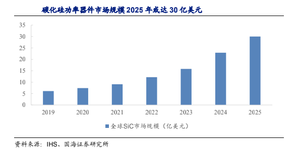
In the past three years alone, as a semiconductor technology, silicon carbide (SiC) has developed to a level that can compete with silicon. Today, silicon carbide has entered the third generation of products, and its performance has increased with more and more applications.
Compared with traditional silicon, SiC has excellent performance
The band gap is wider, the critical breakdown voltage is higher, the electron speed is higher, and the switching speed is faster. For a given rated voltage, the die size can be much smaller, resulting in low on-resistance, coupled with better thermal conductivity, which can reduce losses and lower operating temperature. The smaller die size also reduces device capacitance, thereby reducing switching losses, while the inherent high-temperature performance of SiC reduces thermal stress.
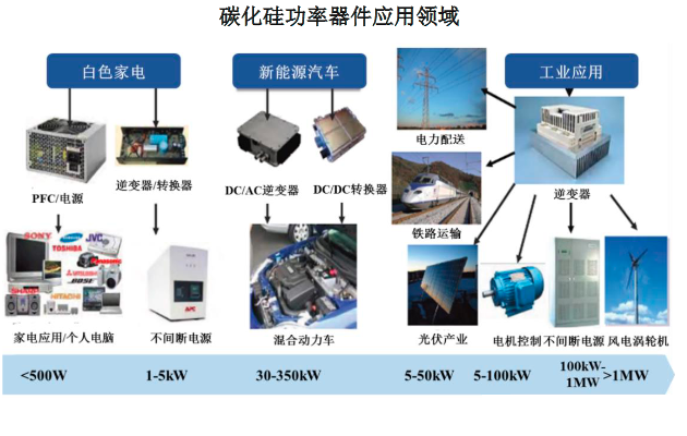
SiC device application field
SiC devices are being widely used in the field of power electronics. Typical markets include rail transit, power factor correction power supply (PFC), wind power (wind), photovoltaic (PV), new energy vehicles (EV/HEV), charging piles, and Discontinuous power supply (UPS), etc.
Among them, new energy vehicles are the main growth point of SiC power devices:
Tesla Model 3 uses SiC MOSFET from STMicroelectronics;
Domestic car companies such as BYD, NIO, Xiaopeng are already adopting silicon carbide. Recently, three more car companies have joined the wave of silicon carbide applications:
Hon Hai (Foxconn): invested nearly 600 million yuan to acquire a 6-inch SiC wafer fab, with an annual production capacity of 180,000 pieces;
Geely: The pure electric platform has adopted Rohm SiC technology, and is also deploying SiC localization;
Zero running: Mass production of 800V SiC electronic control products in 2023.
According to incomplete statistics of the "three-generation half-wind direction", more than a dozen domestic vehicles have already adopted or explicitly stated that they will use silicon carbide. The demand for silicon carbide vehicles is expected to increase rapidly in the next two years.
Test challenges of SiC devices
Driven by the steady growth of the SiC power semiconductor market space, semiconductor performance requirements continue to increase. How to ensure that the selected power devices can operate stably and reliably under high temperature, strong radiation, and high power environments to ensure yield, which brings design engineers Here comes a very big test challenge.
One of the most important equipment in semiconductor testing is the probe station, which is mainly used in the testing of semiconductor industry, optoelectronic industry, integrated circuit and packaging. The probe station is a key equipment for testing the electrical and optical parameters of semiconductor chips. After testing, the probe station records the crystal grains whose parameter characteristics do not meet the requirements, and removes them before entering the subsequent process, which greatly reduces the manufacturing cost of the device.
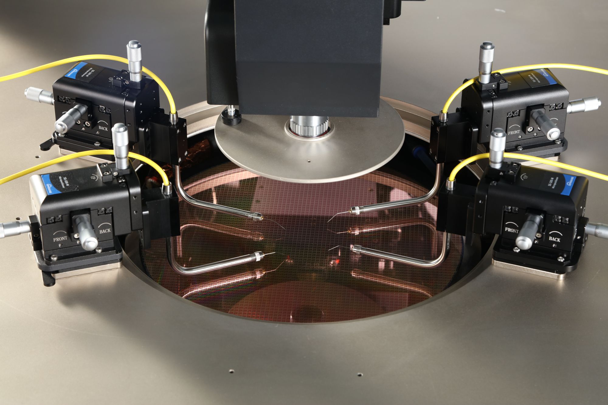
SEMISHARE can provide standardized and customized probe stations. Take SEMISHARE X12 (X Series) as an example. It is a semi-automatic probe station that integrates electrical, light wave, microwave, and other test functions. It is compatible with the performance test of advanced chips of various materials such as 8-inch, 6-inch) Si, GaN, SiC. It can perform 7*24 on-chip detection of wafers, MEMS, biological structures, optoelectronic devices, high-power devices (such as IGBT, MOSFET devices) and other integrated circuits, LEDs, LCDs, solar cells, etc., and can be loaded with temperature control systems , To meet the various performance test requirements of customers in high and low temperature environments. The equipment can be equipped with corresponding instruments and meters to perform characteristic analysis of IV, CV, optical signal, RF, 1/F noise, etc. of various components, wafers, etc. It is a comprehensive multifunctional semi-automatic probe station, and can be based on If necessary, set customized technical indicators to match customers' general equipment requirements.

SEMISHARE's solution
- Reduce the contact resistance from the wafer stage to the back of the wafer
Minimize the contact resistance, that is, minimize the contact resistance between the wafer and the chuck. Broadly speaking, contact resistance refers to the resistance between conductors. The true contact resistance is composed of concentrated resistance, film layer resistance and conductor resistance. There are many factors that affect contact resistance, such as the material of the contact, the force generated by the contact surface and perpendicular to the contact surface, the state of the contact surface, and the magnitude of the applied voltage/current. The SEMISHARE probe station adopts a gold-plated high-power high-temperature stage with a gold-plated surface and evenly distributed porous suction holes, which can protect to thin/warped wafers, and is provided when the user performs vertical component on-resistance RDS(ON) measurement Excellent crystal back contact and low contact resistance at the same time.
- Avoid burning and damage of metal pads of high-current components
By using multi-pin high-current shunt probes, not only the contact resistance of the probes can be reduced, but also the current dispersion can be used to reduce the situation that the metal pads of the components are easily burned during the detection of single-pin probes in the past;
- Low leakage current measurement under high voltage and various temperature conditions
The probe is fixed by the inner copper tube, the outer copper tube is shielded from noise interference, and there is an insulating layer between the inner and outer copper tubes. (You can choose to connect to the back end with ordinary cables, coaxial or triaxial cables.) Suitable for weak current and high voltage; imported high-quality cables, front-end tube-mounted shielding structure, leakage (under normal pressure) <100fA, with shielding The box uses the highest high voltage resistance of 10000V.
- Provide a safe testing environment
Through the use of a safety protective cover (interlock protection function of the operating terminal connection test instrument); at the same time, Chuck is isolated and protected by insulating materials from other metals, which can effectively guarantee a safe test environment.

SEMISHARE is committed to providing customers with high-performance wafer probe stations and test solutions. It currently serves universities and research institutes, integrated circuit FAB, panel manufacturers and other enterprises. As a model of China’s emerging semiconductor test equipment industry, the company is in the field of semiconductor testing. With many successful technical cases and experiences, we will continue to provide accurate, stable and fast test solutions for the industry.