High Voltage Probe Test Solutions for Semiconductors | SEMISHARE
SEMISHARE's cutting-edge semiconductor wafer prober testing solutions and RF test probes are transforming on-wafer testing. Learn about our latest advancements.
High Voltage Probes and Semiconductor Test Solutions: Advancing Precision in Power Electronics
In the rapidly evolving landscape of power electronics, the demand for high voltage probes and comprehensive semiconductor test solutions has never been more critical. As industries like 5G telecommunications, electric vehicles, and renewable energy continue to push the boundaries of semiconductor technology, the need for precise, reliable testing equipment has become paramount. SEMISHARE, a leading innovator in the field, stands at the forefront of this technological revolution, offering cutting-edge high voltage probes and semiconductor test solutions that are reshaping the industry.
The Rise of Third-Generation Semiconductors
The emergence of third-generation semiconductors, particularly Gallium Nitride (GaN) and Silicon Carbide (SiC), has ushered in a new era of high-power, high-efficiency electronic devices. These materials offer superior performance characteristics, including higher voltage tolerance, lower on-resistance, and faster switching speeds. However, with these advancements come new challenges in testing and measurement, requiring sophisticated high voltage probes and semiconductor test solutions to ensure reliability and performance.
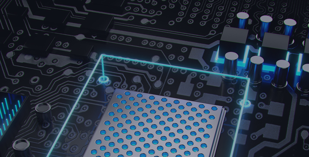
High Voltage Probe: The Cornerstone of Accurate Measurement
A high voltage probe is an indispensable tool in the arsenal of semiconductor testing equipment. These specialized probes are designed to safely and accurately measure voltages in high-power semiconductor devices, providing critical data for engineers and manufacturers.
When should a high voltage probe be used?
High voltage probes are essential when testing devices that operate at voltages exceeding standard measurement equipment capabilities. They are particularly crucial in applications involving power semiconductors, where voltages can reach several kilovolts. Engineers rely on high voltage probes to characterize the performance of GaN and SiC devices under high-stress conditions, ensuring they meet the stringent requirements of modern power electronics.
What is the use of voltage probe?
Voltage probes serve as the interface between high-voltage circuits and measurement instruments. They allow for the safe and accurate measurement of voltage levels that would otherwise be beyond the reach of standard test equipment. In semiconductor testing, voltage probes are used to assess the breakdown voltage, leakage current, and overall electrical characteristics of power devices.
What does a high voltage tester do?
A high voltage tester is a specialized instrument designed to apply controlled high voltage stresses to semiconductor devices while measuring their response. These testers play a crucial role in evaluating the insulation strength, dielectric properties, and overall reliability of high-power semiconductors. By subjecting devices to extreme voltage conditions, high voltage testers help identify potential weaknesses or failure points before they can cause issues in real-world applications.
Semiconductor Test Solutions: Ensuring Quality and Reliability
As the complexity of semiconductor devices increases, so does the sophistication of the test solutions required to evaluate them. SEMISHARE's comprehensive suite of semiconductor test solutions addresses the multifaceted challenges of modern device characterization.
What are the methods of semiconductor test?
Semiconductor testing encompasses a wide range of methodologies, each designed to evaluate specific aspects of a device's performance. Some key methods include:
1. Parametric testing: Measures electrical characteristics such as threshold voltage, leakage current, and breakdown voltage.
2. Functional testing: Evaluates the device's ability to perform its intended functions under various operating conditions.
3. Reliability testing: Assesses the long-term performance and durability of the semiconductor device.
4. Thermal testing: Examines the device's behavior across a range of temperatures, crucial for power electronics applications.
How do you test semiconductor materials?
Testing semiconductor materials involves a combination of electrical, optical, and physical characterization techniques. For high-power semiconductors like GaN and SiC, testing often focuses on:
1. Wafer-level probing to assess electrical properties
2. High-temperature testing to evaluate performance in extreme conditions
3. Breakdown voltage measurements to determine maximum operating limits
4. Switching speed tests to characterize high-frequency performance
What is the testing equipment for the semiconductor industry?
The semiconductor industry relies on a diverse array of testing equipment to ensure the quality and reliability of its products. This equipment includes:
1. Probe stations for wafer-level testing
2. Automated test equipment (ATE) for high-volume production testing
3. Curve tracers for device characterization
4. Thermal chambers for temperature-dependent testing
5. High voltage testers for power device evaluation
SEMISHARE's advanced probe stations and test solutions are designed to meet the specific needs of third-generation semiconductor testing, offering unparalleled precision and reliability.
What is semiconductor automated test equipment?
Semiconductor automated test equipment (ATE) refers to sophisticated systems that perform a wide range of tests on semiconductor devices with minimal human intervention. These systems are capable of conducting complex test sequences, collecting data, and analyzing results at high speeds, making them essential for large-scale semiconductor production.
SEMISHARE's automated test solutions incorporate cutting-edge technology to streamline the testing process, improve accuracy, and increase throughput. Our ATE systems are designed to handle the unique challenges posed by high-power semiconductors, ensuring comprehensive testing across a wide range of parameters.
Semiconductor Testing Equipment Manufacturers: Driving Innovation
As a leading manufacturer of semiconductor testing equipment, SEMISHARE is committed to driving innovation in the industry. Our expertise in high voltage probes and semiconductor test solutions positions us at the forefront of technological advancement.
SEMISHARE's Product Offerings
1. High Voltage Probes: Our advanced high voltage probes are designed to withstand extreme voltages while providing accurate measurements. These probes feature innovative insulation technologies and precision-engineered tips to ensure reliable contact with semiconductor devices.
2. Probe Stations: SEMISHARE offers a range of probe stations tailored for high-power semiconductor testing. Our stations incorporate advanced features such as thermal management systems, EMI shielding, and high-precision positioning mechanisms.
3. Automated Test Systems: Our ATE solutions combine flexibility with high-throughput capabilities, allowing for efficient testing of a wide range of semiconductor devices. These systems are equipped with user-friendly interfaces and powerful data analysis tools.
4. Custom Test Solutions: Recognizing the unique needs of different semiconductor applications, SEMISHARE provides custom-designed test solutions that address specific challenges in GaN and SiC device characterization.
The SEMISHARE Advantage
1. Expertise in Third-Generation Semiconductors: Our deep understanding of GaN and SiC technologies allows us to develop test solutions that address the specific challenges of these advanced materials.
2. Commitment to Innovation: SEMISHARE invests heavily in research and development, continuously improving our high voltage probes and semiconductor test solutions to meet the evolving needs of the industry.
3. Comprehensive Support: We offer extensive technical support and training to ensure our customers can fully leverage the capabilities of our testing equipment.
4. Quality Assurance: All SEMISHARE products undergo rigorous quality control processes, ensuring reliability and accuracy in every test scenario.
5. Global Presence: With a worldwide network of support and service centers, SEMISHARE provides localized assistance to customers across the globe.
As the semiconductor industry continues to push the boundaries of power electronics, the importance of high voltage probes and comprehensive test solutions cannot be overstated. SEMISHARE's cutting-edge technologies and unwavering commitment to quality position us as a trusted partner in the advancement of semiconductor testing.
By providing state-of-the-art high voltage probes, automated test equipment, and custom solutions for third-generation semiconductors, SEMISHARE enables manufacturers to ensure the reliability, performance, and safety of their power electronic devices. Our innovative approach to semiconductor testing is helping to shape the future of industries ranging from electric vehicles to renewable energy systems.
For those seeking to stay at the forefront of semiconductor technology, partnering with SEMISHARE offers access to the most advanced testing capabilities available. Together, we can drive forward the next generation of power electronics, unlocking new possibilities in efficiency, power density, and performance.
To learn more about how SEMISHARE's high voltage probes and semiconductor test solutions can benefit your organization, visit our website at https://www.semishareprober.com/. Discover the difference that precision, reliability, and innovation can make in your semiconductor testing processes.
With the rise of 5G base stations, new energy vehicles, fast charging and photovoltaic applications, the third generation of high-power semiconductors represented by GaN and SiC are widely used in these hot industries because of their excellent performance, and their high withstand voltage, low on-resistance, and fast switching speed bring higher challenges to wafer-level measurements.

Driven by the steady growth of the power semiconductor market space, the semiconductor performance requirements continue to increase, how to ensure that the selected power devices can operate stably and reliably in high temperature, strong radiation, high power environment to ensure yield, which brings very large test challenges to design engineers.
One of the important equipment in semiconductor testing is the probe station, which is mainly used in the semiconductor industry, optoelectronic industry, integrated circuits and packaging and testing. The main function of the probe station is to test the grain parameter characteristics and classify them for subsequent screening.
The main test objects of high power:
High-power diodes, MOS tubes, IGBTs and other discrete devices, etc
Device Forward Operating Status:
Low voltage, high current, high current state produces high temperature
Device Cut-Off Status:
High voltage, low current, no high temperature in the cut-off state
Test purpose: forward and reverse IV, CV test
Other needs: 10KV, 500A pulse current, high and low temperature, automatic, short circuit protection, personnel high voltage protection, thermal resistance test
When the high voltage and high current test, the more difficult is the high voltage, the high voltage will produce breakdown phenomenon, the occurrence of a relatively large leakage current, so the high voltage on the leakage of electricity requirements are relatively high, to prevent ignition. The cause of the high-voltage test ignition: the air collides and ionizes under the action of the electric field, resulting in a penetrating discharge between the electrodes. At the same time, the air is heated and the temperature rises sharply to create an arc.
How to avoid high-pressure ignition (Figure 1): Point B is 1 standard atmospheric pressure. To improve the ability to withstand breakdown voltage, option one can go in the positive direction of point B (increasing the pressure), or plan two, go in the negative direction of point A (reduce the pressure).

High power high and low temperature test probe station case
Positive pressure working principle: dry air /N2/SF6 with a pressure of more than 5 bar to keep wafer dry, so as to avoid discharge, ignition and other phenomena.

• Maximum voltage 10Kv, maximum current 500A
• 6" to 12" in, manual/semi-automatic/fully automatic
• -60℃~200℃
• mΩ class chuck contact resistance
• Support flake, taiko, warped wafer test
• Full range of high pressure and high flow probes
• High-performance enclosed darkroom effectively shields EMI, light and noise while keeping the sample at low temperatures without frost formation in a dry positive pressure environment
• The chamber structure optimized by the darkroom can greatly reduce dry gas consumption
High-power vacuum test probe station example
Vacuum working principle: vacuum insulation arc extinguishing technology, the use of high vacuum, generally 10-2~ 10-5Pa, the insulation strength of the vacuum gap at this time is much higher than the insulation strength of 1 atmosphere of air and SF6, higher than the insulation strength of transformer oil. All clearances can be made small.

• Can support 4.2K-450K temperature
• Radiation-proof screen design to improve sample temperature uniformity and accuracy
• Probe heat sink design ensures accurate needle drop
• Upgradable loading magnetic field
• Flexible and scalable test application configuration
• Automatic refrigerant flow control, automatic and precise temperature control
2022.12.7-9, SEMISHARE will attend the 4th Shenzhen International Semiconductor Exhibition, Address: Shenzhen International Convention and Exhibition Center (Baoan New Pavilion). Our booth number: Hall 12, 4A013.
We look forward to your visit and face-to-face communication and discussion with our engineers!