

Efficient, accurate, and low-cost wafer-level testing is a major bottleneck for scaling silicon photonics production. SEMISHARE's new Wafer-Level Silicon Photonics Test System tackles this challenge head-on. It combines advanced coupling technology with sub-micron precision positioning and versatile calibration to enable fast switching between test modes. This solution drastically cuts test time and enhances yield analysis accuracy for equipment manufacturers.

Intelligent hand-eye coordination
The system is equipped with a high-precision six-axis displacement stage and a piezoelectric ceramic platform, supporting fixed-point rotation optimization to ensure the optimal coupling path for the beam, focus, and optical axis, thereby addressing complex spatial trajectories. The coupling system utilizes real-time feedback and intelligent algorithms to optimize alignment paths, achieving sub-micron precision positioning and locking onto the optimal coupling position. This enables a perfect balance between efficiency and accuracy.
Compatible with multiple coupling methods, it's adaptable to various test scenarios
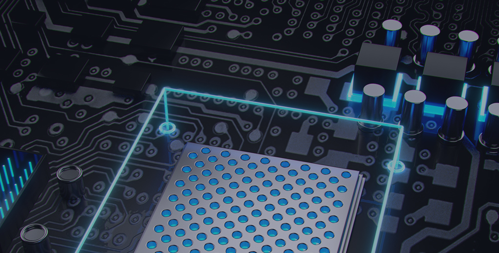
The system comprehensively supports edge coupling, wafer-level edge coupling, and vertical coupling methods, and is compatible with various coupling structures ranging from single fiber to fiber arrays, meeting requirements for different polarizations, bandwidths, and integration levels.
• Edge Coupling Solution: For designs prioritizing low loss, broad spectrum, and polarization insensitivity, we provide an automated edge alignment solution. It specifically supports wafer-level edge coupling, enabling high-precision XYZ alignment and UVW angular alignment of fiber arrays (FA) with array waveguides within microgrooves with depths ≥50 μm and widths ≥100 μm. This addresses the process challenges of wafer-level batch testing.
• Vertical Coupling Solution: Utilizing grating structures, this solution achieves vertical optical coupling on the chip surface. It is particularly suitable for wafer-level testing and three-dimensional high-density integration. Coupling gratings can be positioned anywhere on the chip, offering significant convenience for automated batch testing.

Intelligent Software: The "Brain" of Test Automation
The wafer-level silicon photonics testing software deeply integrates the machine vision and optical positioning of the probe station with the six-axis coupling system. Through a graphical interface, users can effortlessly perform operations such as optical alignment verification, wafer training, and measurement position training. This automates the complex multi-degree-of-freedom alignment process, significantly lowering the operational barrier while enhancing the consistency and repeatability of testing.

PTS™ Integrated Test System supports both engineering and mass production requirements
Designed specifically for engineering and mass-production clients, it supports:
•Multi-instrument integration and multi-site parallel testing;
•Separation of test procedures and platforms, enabling secondary development;
•Raw data storage, automated analysis, and generation of customized reports;
•User-customizable UI interfaces and test workflows

Flexible Fixture Solutions for Multi-Model Testing
SEMISHARE offers a range of customized fixtures (horizontal, wafer-level, and vertical coupling fixtures), supporting single fibers and fiber arrays with various offset angles and dimensions to meet both horizontal and vertical coupling requirements.
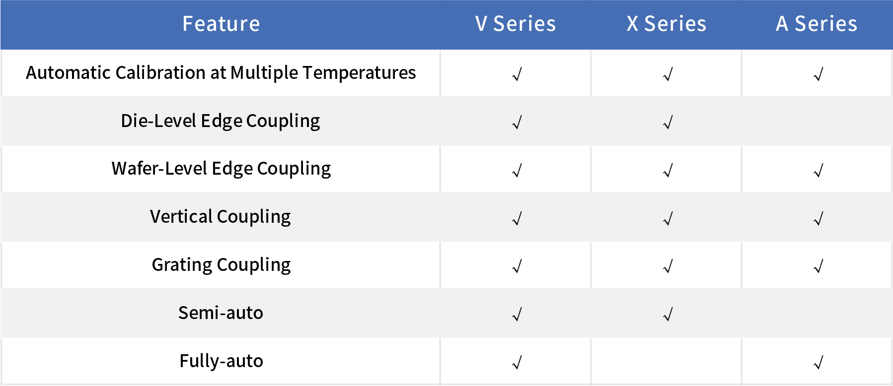
When it comes to probe station pairing, users can freely select SEMISHARE's V-Series, X-Series, or A-Series probe stations according to their specific needs, ensuring flexible adaptation to diverse laboratory and production line environments.
Compatible Models
Relying on stable and reliable hardware design and intelligent operation logic, the SEMISHARE Wafer-Level Silicon Photonics Test System has been validated by multiple silicon photonics module manufacturers. It effectively increases test throughput and reduces overall costs, providing solid support for the large-scale commercialization of silicon photonic devices.