Exploring News in Failure Analysis - SEMISHARE Prober
Stay informed about failure analysis at SEMISHARE Prober's trade shows. Discover insights, technologies, and trends shaping the future of semiconductor testing.
SEMISHARE: Pioneering Advanced Failure Analysis in Semiconductor Manufacturing
In the intricate world of semiconductor manufacturing, where precision and reliability are paramount, the ability to quickly and accurately diagnose issues is critical. This is where failure analysis comes into play, a process essential for ensuring product quality and reliability. SEMISHARE, a leading provider of semiconductor testing solutions, offers a comprehensive approach to failure analysis that incorporates a variety of cutting-edge methods and tools.
Understanding Failure Analysis in Semiconductor Manufacturing
Failure analysis in the semiconductor industry is a multifaceted process that involves identifying, characterizing, and determining the root causes of failures in semiconductor devices. This critical process helps manufacturers improve product reliability, enhance yield rates, and optimize manufacturing processes.
The FMEA Process: A Systematic Approach to Failure Prevention
The Failure Modes and Effects Analysis (FMEA) process is a proactive methodology used in semiconductor manufacturing to identify potential failure points before they occur. SEMISHARE's implementation of FMEA involves several key steps:
1. Potential Failure Mode Identification: Our experts systematically analyze each component and process step to identify possible ways in which a failure could occur.
2. Effect Severity Assessment: We evaluate the potential impact of each failure mode on the device's performance, reliability, and user experience.
3. Cause Determination: Our team investigates the underlying causes that could lead to each failure mode, considering factors such as design flaws, process variations, and material defects.
4. Occurrence Likelihood Estimation: We assess the probability of each failure mode occurring based on historical data and industry knowledge.
5. Detection Method Evaluation: Our analysts review existing quality control measures to determine how effectively potential failures can be detected before reaching the end-user.
6. Risk Prioritization: By combining severity, occurrence, and detection ratings, we calculate a Risk Priority Number (RPN) for each potential failure mode.
7. Mitigation Strategy Development: Based on the RPN, we develop and implement strategies to reduce the risk of high-priority failure modes.
8. Continuous Monitoring and Improvement: Our FMEA process is ongoing, with regular reviews and updates to ensure its effectiveness in preventing failures.
Process Failure Analysis: Uncovering the Root of Manufacturing Issues
Process failure analysis is a critical component of SEMISHARE's comprehensive failure analysis approach. This in-depth examination of manufacturing processes helps identify the root causes of defects or failures. Our process failure analysis includes:
1. Process Mapping: We create detailed flowcharts of the manufacturing process to visualize each step and identify potential failure points.
2. Data Collection and Analysis: Our team gathers and analyzes process data, including equipment parameters, material specifications, and environmental conditions.
3. Statistical Process Control: We employ advanced statistical techniques to identify trends and anomalies in the manufacturing process.
4. Failure Mode Correlation: Our experts correlate observed failures with specific process steps or parameters to pinpoint areas for improvement.
5. Root Cause Analysis: Using techniques such as the "5 Whys" and Ishikawa diagrams, we drill down to the fundamental causes of process failures.
6. Corrective Action Implementation: Based on our findings, we develop and implement targeted improvements to prevent recurrence of identified issues.
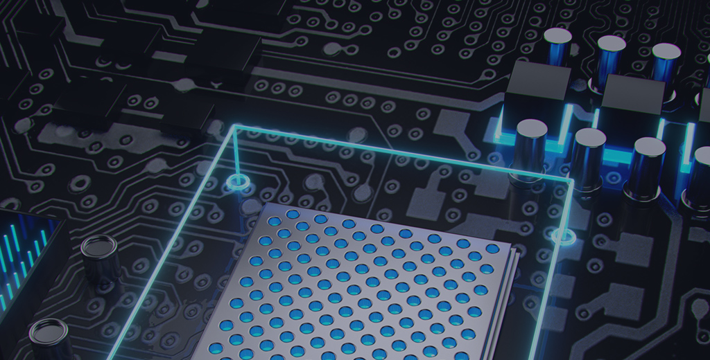
Advanced Tools for Comprehensive Failure Analysis
SEMISHARE utilizes a wide array of sophisticated tools for failure analysis, each serving a specific purpose in uncovering the mysteries of semiconductor failures:
1. Optical Microscopy (OM): Our high-resolution optical microscopes provide initial visual inspection, allowing for quick identification of surface defects and anomalies.
2. Ultrasonic Scanner Microscope (C-SAM): This non-destructive tool allows us to examine internal structures, identifying issues like delamination or voids without damaging the sample.
3. X-ray Imaging: Our advanced X-ray systems reveal hidden defects within packaged devices, such as wire bond issues or solder joint problems.
4. Scanning Electron Microscope (SEM) with Energy-Dispersive X-ray (EDX) Spectroscopy: This powerful combination allows for high-magnification imaging and elemental analysis, crucial for identifying contaminants or material defects.
5. Focused Ion Beam (FIB) Systems: These versatile tools enable precise cross-sectioning and circuit modification, allowing for in-depth analysis of specific areas of interest.
6. Emission Microscopy (EMMI): We use this technique to detect and localize areas of abnormal current flow, which can indicate potential failure sites.
7. Time-Domain Reflectometry (TDR): This method helps us identify discontinuities in high-speed signal paths, crucial for analyzing failures in advanced semiconductor devices.
8. Laser Voltage Probing (LVP): This non-contact technique allows us to measure voltage levels at internal nodes of a device, providing invaluable information about its electrical behavior.
Test Failure Analysis: Bridging Design and Manufacturing
Test failure analysis is a critical process that links device design with manufacturing outcomes. SEMISHARE's approach to test failure analysis includes:
1. Parametric Test Analysis: We meticulously examine device parameters to identify deviations from expected values.
2. Functional Test Evaluation: Our team analyzes the results of functional tests to pinpoint specific operational failures.
3. Burn-in Test Assessment: We review data from accelerated life tests to identify reliability issues that may not be apparent in standard testing.
4. Environmental Test Analysis: Our experts evaluate device performance under various environmental conditions to ensure robustness in real-world applications.
5. Electrical Characterization: We perform detailed electrical measurements to understand the device's behavior under various operating conditions.
6. Failure Signature Identification: By analyzing test data patterns, we can often identify specific failure mechanisms or manufacturing issues.
SEMISHARE's Comprehensive Chip Failure Analysis Methodology
Our approach to chip failure analysis is designed to be thorough and efficient, leveraging a wide range of techniques to ensure no potential failure mechanism is overlooked:
1. Initial Non-Destructive Analysis:
- Optical Microscopy for surface inspection
- X-ray imaging for internal structure examination
- C-SAM analysis for detecting internal defects without damage
2. Electrical Characterization:
- I-V curve analysis
- Parametric testing
- Functional testing under various conditions
3. Advanced Physical Analysis:
- SEM/EDX for high-resolution imaging and elemental analysis
- FIB for precise cross-sectioning and circuit modification
- EMMI for detecting areas of abnormal current flow
4. Specialized Techniques:
- Laser cutting for sample preparation
- Layer removal using RIE or chemical etching
- Probing and electrical testing at the die level
5. Reliability Assessment:
- ESD testing to evaluate device susceptibility to electrostatic discharge
- Latch-up testing to assess vulnerability to parasitic effects
By employing this comprehensive suite of failure analysis techniques, SEMISHARE ensures that our clients receive the most accurate and actionable insights into device failures, enabling them to improve their products and processes continuously.
SEMISHARE's Commitment to Excellence in Failure Analysis
In the fast-paced and highly competitive semiconductor industry, the ability to quickly and accurately diagnose and resolve issues is a key differentiator. SEMISHARE's advanced failure analysis capabilities, spanning from proactive FMEA to in-depth chip-level analysis, provide our clients with the tools and expertise needed to stay ahead in this challenging field.
Our commitment to continuous improvement and investment in cutting-edge technologies ensures that we remain at the forefront of semiconductor failure analysis. By partnering with SEMISHARE, semiconductor manufacturers gain access to a wealth of knowledge and resources that can help them improve product quality, increase yield rates, and accelerate time-to-market for new devices.
Whether you're dealing with a specific device failure or looking to enhance your overall quality assurance processes, SEMISHARE's comprehensive failure analysis services can provide the insights you need to succeed. Visit our website at https://www.semishareprober.com/ to learn more about how our advanced failure analysis capabilities can benefit your semiconductor manufacturing operations.
Chip failure analysis method:
1.OM microscope observation and appearance analysis
2. C-sam (ultrasonic scanner microscope)
(1) Structure of lattice constant inside the raw materials, residuals, ginseng and sundries, precipitation,
((2) Internal cracks. (3) Hierarchical defects. (4) Cracks, bubbles, gaps, etc.。
3. X-ray detects various defects in IC packaging, such as layer disconnection, crack, crack and wiring consistency, defects in PCB soldering, such as poor center or bridging, defects in lead, short circuit fault or abnormal connection, and consistency of tin ball in packaging. (These are the first non-destructive analysis methods used after a chip is invalidated.)
4.4.SEMsem/EDX kinetic dispersive X-ray apparatus (structural analysis of raw materials/observation of defects, analysis of basic micro area of element composition, specification of side electronic devices)
5.Take DIE, the laser and acid opener are used in Kaifeng city to remove the shell part of the tested sample (not suitable for porcelain and metal packaging), so as to expose the internal structure of the tested sample.
6. EMMI low light level microscope /OBIRCH laser beam induced characteristic impedance value transformation detection /LC LIQUID crystal display network hot spot detection (these three belong to the common leakage current path analysis means, and LC relies on probe table and digital oscilloscope to find the network hot spot)
7.Laser cutting sample making: The control module of laser cutting sample making is used to fix the small sample, so as to facilitate the afterwards test
8.Layer removal: RIE is used to remove the passivation layer inside the chip to expose the metal material of the next layer of the sample. If the structure of the next layer is to be examined by removing the metal material layer, grinding equipment can be used to remove the layer.
9.FIB to do some power circuit changes, cut point inspection
10. The Probe Station prober/Probing Test electrode.
11.ESD/Latch-up ELECTROSTATIC discharge/latching effect detection (some customers perform these two reliability tests before the chip is injected into the mobile phone client, and some customers think of screening the good film after it is invalid), which has been mentioned for most common methods.
Nothing but common methods also have some other means of failure analysis, atomic force microscope AFM, secondary positive ion mass spectrometry SIMS, aviation tof-sims time mass spectrometry analysis, transmission electron microscopy, TEM, send electron microscopy (sem), send the scanner auger electrode, X-ray photoelectron spectroscopy (XPS, L - I - V test system software, the kinetic energy damage many means such as X-ray microanalysis system software, but this new project is not very common.
Failure analysis of China software Detection chip
Chip failure analysis process:
1.I usually do a physical first to see if there's crack or Burnt mark or anything else;
2.Non-destructive analysis: The key is xRay -- look at the internal configuration, ultrasonic scanner microscope (C-SAM)-- see without delaminaTIon, these;
3.Electrical measuring system: key special tools, IV, digital multimeter, digital oscilloscope, SONY TEK370B;
4.Destructive analysis: Mechanical equipment DECAP, organic chemistry DECAP chip opener
Chip failure analysis Laboratory details:
Analysis communication soft detection, intelligent household product testing laboratories can according to the international, China and the national standards for testing work, from the bottom of the chip to actually goods, from physics to the logic of a full range of testing work, produce the wireless chip preparation processing, side channel attack, attack, invasion type attack, natural environment, the working voltage flash attack, electromagnetic induction introduction, rays, introducing, physical security and logical security, function and compatibility mode and introduce a little bit more laser safety testing services, in addition to simulation reproduce the situation of smart home products is invalid, The failure analysis and detection service items for the cause of invalidation were found, including point-pin service center, RIE, EMMI, X-ray detection, FIB system software and other detection experiments. Maintain quality assessment and analysis of intelligent products, and show quality commitment for chip, embedded software and application of precision machinery products.