Semiconductor laser chips can be divided into Vertical Cavity Surface Emiting Laser (VCSEL) and Edgc-Emitting Laser (EEL) according to the direction of light emission. VCSEL is widely used in laser communication and display fields because of its good beam quality and high frequency. But the relatively low power is an important limiting factor. Therefore, high-power semiconductor lasers usually choose edge-emitting chips.
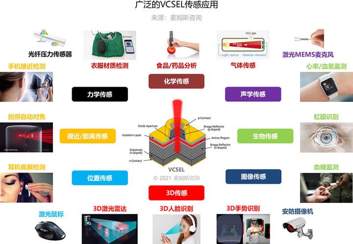
VCSEL sensing application
In 2004, VCSEL entered consumer electronics products for the first time: Logitech MX1000 laser wireless mouse, which became the light source of laser navigation (positioning) sensors. In 2017, the VCSEL array entered Apple iPhone X for the first time and became the light source for 3D face recognition. This has also ignited the entire VCSEL industry, and the market scale has expanded rapidly. VCSEL technology is currently attracting attention in application fields such as face recognition, 3D sensing, auto-driving cars, gesture detection, and VR (virtual reality)/AR (augmented reality)/MR (mixed reality).
the advantage of VCSEL
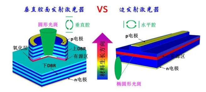
1. The exit spot is circular, as shown on the left side of the figure below, while the exit spot of EEL is elliptical. The circular spot of VCSEL is easier to couple with the fiber, and the coupling efficiency is much larger than that of EEL.
2. The light emitting direction of VCSEL is vertical, while EEL emits light from the side. VCSEL emits light vertically, which is more suitable for making a two-dimensional array.
3. The VCSEL threshold current is very small, and it can work at a low current between 1 and 2 mA, with low energy consumption
4. The VCSEL can test the chip before packaging and screen the product, which greatly reduces the cost of the product. For EEL, the wafer must be cut, and then the rest of the device must be constructed and tested. Make testing more difficult.
Test and analysis of VCSEL wafer optical parameters
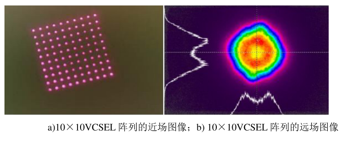
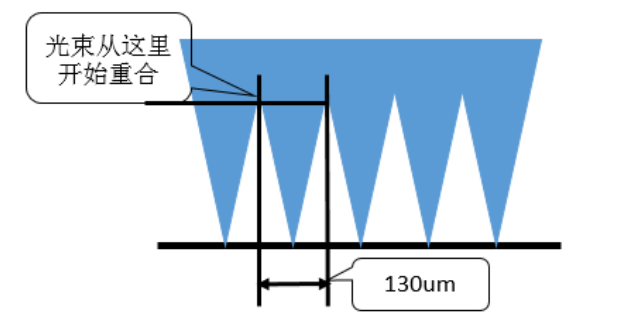
Assuming that the center-to-center distance of each unit is 130μm, the area of each unit is 130μmx130μm square. Since each VCSEL unit has a certain divergence angle, the beam diameter of each unit will increase with the increase of the propagation distance. After the beam travels for a certain distance, the beams will start to coincide, and the diameter of the coincident light spot will start to be greater than 130 microns. The greater the divergence angle of the light beam, the shorter the distance at which the light beams start to coincide. Before the beams coincide, the obtained light intensity distribution is a near-field image, and the image is the light spot of each VCSEL unit. After a long distance propagation, the light spots of each VCSEL unit begin to overlap, and we get the far-field image of the VCSEL array.
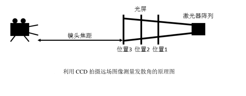
We obtained the near-field image of the VCSEL array by taking a photomicrograph, and obtained the far-field image of the VCSEL array by taking the image on the light screen by a CCD camera. The following figure is a schematic diagram of using a CCD camera to take a far-field image. The distance between the light screen and the CCD camera is the focal length of the lens. At this time, the image on the light screen is reduced by the lens by a fixed multiple and then projected onto the photosensitive original, so that not only the light of the spot can be measured Strong distribution can also measure the size of the spot, so we can measure the divergence angle of the VCSEL array through this system. It should be noted that when measuring the spot size at different positions, it is necessary to ensure that the relative position of the light screen and the lens is unchanged, otherwise the light screen will not be in the focal plane of the lens. This measurement result is inaccurate, so we can move Laser array or moving light screen and CCD lens at the same time.
he far-field image mainly reflects the intensity distribution and divergence angle of the beam of the VCSEL array. For VCSEL arrays, near-field images can help us determine whether there are damaged cells in the VCSEL array.
The following pictures are the images taken by the near-field camera and the far-field camera.