Product Overview
X series is an integrated and highly efficient semi-automatic wafer probe platform that is specialized in testing the performance of various advanced chips. It integrates various functions such as electric light wave and microwave, etc. It has the highest temperature width and test accuracy in the industry at present, and can match various test application environments, providing reliability wafer testing within -60 ~300 wide temperature range. ***Custom design solutions for special dimension or performance are possibile on request***
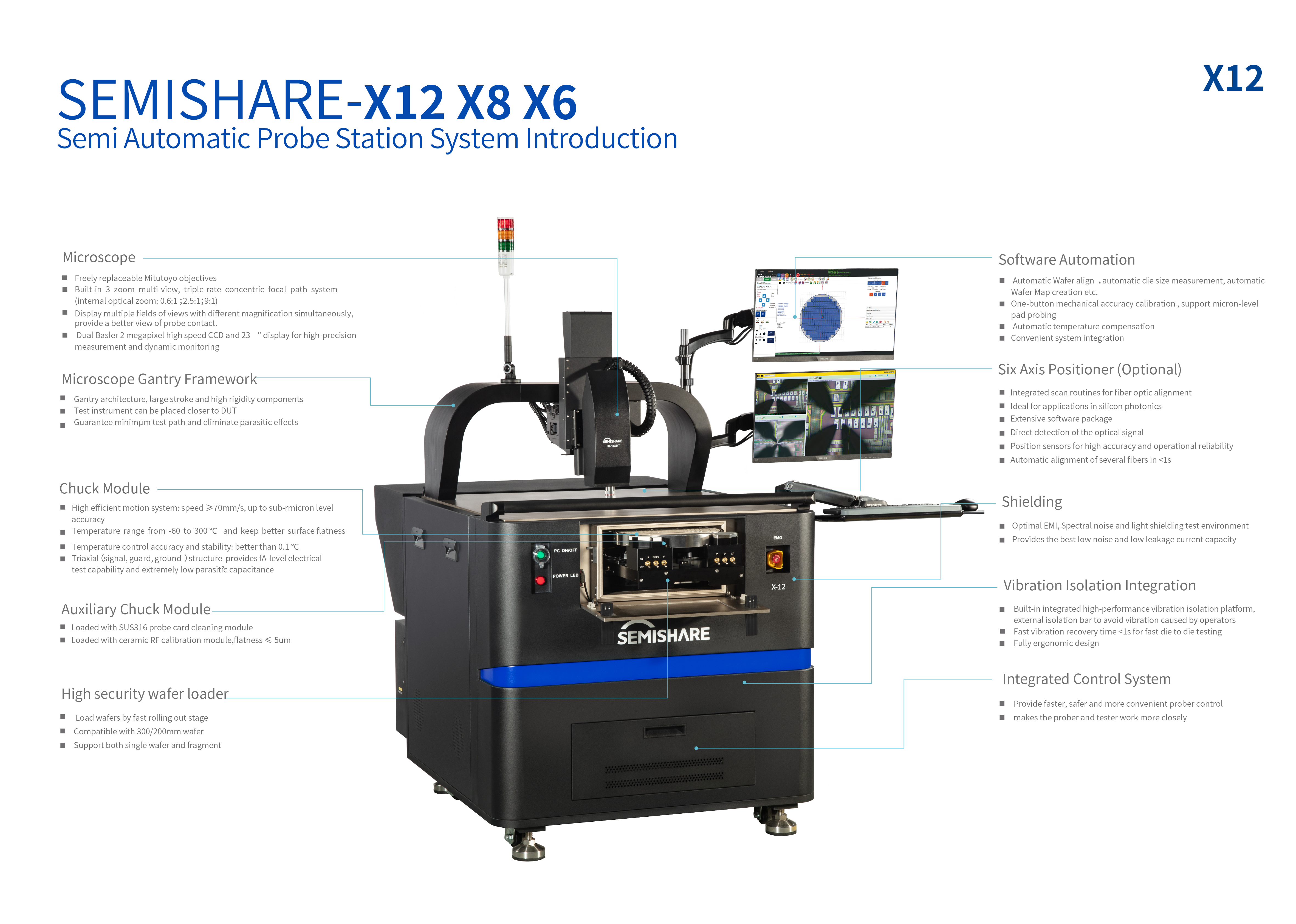
Basic Information
| Product number | X6/X8/X12 | working environment | Open type |
| electricity demand | 220V,50~60Hz | Control method | Semi-Automatic |
| Product Size | 1060mm*1610mm*1550mm | equipment weight | About 1500 kg |
Application direction
Equipment professional deal with 12 "8" 6 "wafer Si/GaN/SiC and other kinds of devices of advanced chip performance test, can be equipped with corresponding instruments and meters, for the I - V C - V light RF signal character such as 1 / f noise analysis, feature-rich devices, scalable high-power wafer test RF test automatic test, and can load temperature control system, satisfy the customer in the high and low temperature environment of all kinds of wafer device performance test requirements.
Technical characteristics
The industry's most efficient CHUCK system, test efficiency increased by more than 40%
● The industry's most efficient CHUCK test system running speed & GT;70mm/s, motion precision 1 m, while moving the translocation time index time 500ms, excellent system operating parameters have reached the highest level of the industry, ultra-high test accuracy and efficiency to meet all kinds of wafers and devices of high repeatability and stability test, compared with other probe brands in the industry, the test efficiency is effectively increased by more than 40%. ●-60 ~300 is the highest temperature wide area in the industry, with temperature control accuracy and stability better than 0.08, providing reliability wafer testing in high and low temperature environments. ●The compact structure design of four-dimensional motion with low center of gravity ensures the motion speed of 70mm/s while maintaining the stability of motion acceleration and deceleration.
Industry leading 3 times imaging technology
Built-in SEMISHARE patent more than three zoom microscope view three times with JiaoGuang road system, 120 x 2000 x variable times optical amplifier, size view shows at the same time, more can make the point needle and convenient operation, double Basler 2 million pixels high speed CCD 23 "display and Mituyoyo high precision high resolution camera, precision positioning of high stability high definition, image output and high precision measurement and dynamic monitoring.
Auxiliary CHUCK module silicon wafer safe upper and lower
●The unique Chuck XY axis design in the industry has changed the common phenomenon that the probe system of other brands in the market is affected by the resistance of laminated plates in different directions and sizes, leading to the decline of motion stability.This ensures that the XY axis is not affected by the laminate when moving, making the motion precision and stability higher. ●Compared with other brands in the industry, the probe table cavity of SEMISHARE can be opened once and pulled out the entire Chuck mechanism to load and load silicon wafers at a speed of 370mm with a long stroke. The manual feeding of the Wafer is more convenient and faster.Meanwhile, the Chuck's rotation Angle range is larger, which requires lower demand for manual laying wafer, and the operation is more flexible and convenient.
Design of O-type needle seat platform
The probe testing system adopts the O-type needle seat platform design, which makes the most efficient use of the space of the needle seat, up to 12 needle seats can be placed at the same time. Compared with other probe brands in the market, the number of the needle seat is increased by 50%, effectively realizing more efficient and rapid testing.
Air film shock absorption system
The industry's unique internal integration of high-performance air film shock absorption system and the dual design of the external isolation barrier, effectively avoid the vibration caused by the operator's touch;In addition, a long-aging casting is used as the substrate to suppress the vibration in the process of motion at the fastest speed of 1S in the industry to ensure the stable operation of the equipment, and to ensure that the screen does not shake when the image is enlarged at 2000X;At the same time, the high-precision control valve ensures that the height error of the moving part of the platform is 0.1mm, effectively realizing the test ability of fast DIE to die, ensuring that the whole system can still maintain a stable running state when moving at a high speed, and greatly improving the test efficiency.
Anti-interference shielding system
Anti interference EMI/Spectral noise/external light closed shielding cavity, cavity with the surface of conductive oxide and nickel plating process, to ensure the conduction state between the parts so as to achieve the shielding effect, reduce the system noise, blocking interference effectively, and provide low leakage current protection, provides the best test environment for the weak electric signal test;At the same time, the closed chamber in the low temperature environment to avoid the test sample condensation, to ensure the wafer and device under the high and low temperature environment fast and safe reliability test.
Independent research and development of software integration system, more compatibility
●Support semi-automatic control (manual test or automatic test). ●Automatic Wafer calibration automatic Wafer mapping automatic die size measurement automatic align automatic test data can be accessed remotely. ●Automatic calibration of RF probe module with one key, automatic needle clearing function. ●One-key adaptive four-axis Chuck precision calibration, supporting micron pad point measurement. ●Single point or continuous testing can be supported. ● Strong data storage capacity and data processing capacity. ●The bin value can be divided to determine the device NG. ●Multi-system integration to upgrade the operating system application system and device test system independently. ●Intuitive and simple operation design, quick and easy operation, effective saving operation training time.
Flexible optional configuration and extension
Convenient instrument access and support system automatic expansion and upgrade, temperature control system loading;There are also a variety of test modules available. According to the test module, it can be used together with a variety of positioner fixtures, needle CARDS and probe tables, such as six-axis positioner RF cables.Many system operating parameters and features reach the highest level of the industry, can meet your different test needs, but also an ideal choice for more industry customers a semi-automatic probe table equipment.