auto prober/Automatic Prober/Probe Stations at SEMISHARE Prober
auto prober/Automatic prober/probe stations of SEMISHARE Probe are designed to revolutionize your semiconductor testing processes , 24*7 on-wafer detection.
SEMISHARE: Revolutionizing Semiconductor Testing with Advanced Automatic Probe Stations
In the ever-evolving landscape of semiconductor manufacturing, the demand for precise, efficient, and reliable testing solutions has never been greater. SEMISHARE stands at the forefront of this technological revolution, offering cutting-edge automatic probe stations that are reshaping the industry. Our commitment to innovation is evident in our state-of-the-art aotomatic prober, automatic probe station, and auto prober technologies, which are designed to meet the most stringent demands of modern semiconductor testing.
Understanding the Role of Probers in Semiconductor Testing
What does a prober do? At its core, a prober is a sophisticated device used in semiconductor testing to establish electrical contact with a wafer or die, enabling the measurement of its electrical characteristics. This crucial tool plays a pivotal role in evaluating the performance and functionality of semiconductor devices, ensuring that each chip meets the rigorous standards required by the industry.
The aotomatic prober developed by SEMISHARE takes this concept to new heights, offering unparalleled precision and efficiency in semiconductor testing. Our aotomatic prober integrates advanced automation technologies with high-precision measurement capabilities, allowing for rapid and accurate testing of complex semiconductor devices.
Advancing Semiconductor Testing with SEMISHARE's Aotomatic Prober
SEMISHARE's aotomatic prober represents a significant leap forward in semiconductor testing technology. This advanced system combines the precision of traditional probing techniques with the efficiency of automation, resulting in a testing solution that is both highly accurate and incredibly fast.
Key features of our aotomatic prober include:
1. Advanced Pattern Recognition: The aotomatic prober utilizes sophisticated image processing algorithms to accurately locate and align with test pads, even on the most complex chip designs.
2. Multi-Site Testing Capabilities: Our aotomatic prober can simultaneously test multiple dies on a wafer, significantly increasing throughput without compromising accuracy.
3. Intelligent Probe Tip Cleaning: The aotomatic prober incorporates an automated cleaning system that maintains probe tip integrity, ensuring consistent results throughout long testing sessions.
4. Adaptive Testing Algorithms: The software controlling our aotomatic prober can adjust testing parameters in real-time based on initial results, optimizing the testing process for each unique device.
5. Comprehensive Data Analysis: Integrated with powerful analytics tools, our aotomatic prober provides in-depth insights into device performance, helping identify trends and potential issues early in the production process.
The Purpose and Functionality of Probe Stations
The purpose of a probe station extends beyond simple electrical contact. These sophisticated systems provide a stable and accurate platform for comprehensive semiconductor wafer testing. SEMISHARE's automatic probe station is designed to conduct a wide array of tests, including I-V, C-V, RF, and noise measurements, ensuring the quality and reliability of semiconductor devices at every stage of production.
Our automatic probe station is engineered to offer:
1. High-precision measurements across a wide range of parameters
2. Stable testing environment with minimal electromagnetic interference
3. Flexibility to accommodate various wafer sizes and types
4. Integration with advanced data analysis and reporting tools
The Evolution of Auto Prober Technology
SEMISHARE's auto prober technology has evolved significantly over the years, keeping pace with the rapid advancements in semiconductor design and manufacturing. Our latest auto prober systems incorporate cutting-edge features that address the challenges of testing increasingly complex and miniaturized devices.
Some of the key advancements in our auto prober technology include:
1. Nanometer-scale Positioning: Our auto prober systems now offer positioning accuracy down to the nanometer level, crucial for testing the latest generation of semiconductor devices.
2. Advanced Materials Handling: The auto prober incorporates new materials and designs that minimize thermal expansion and vibration, ensuring stable and repeatable measurements.
3. AI-Driven Test Optimization: Leveraging artificial intelligence, our auto prober can learn from previous test results to optimize test sequences and parameters, improving both speed and accuracy.
4. Enhanced Parallelism: The latest auto prober designs allow for even greater parallelism in testing, with some models capable of testing dozens of dies simultaneously.
5. Improved Environmental Controls: Our auto prober systems now offer more precise control over temperature and humidity, critical for ensuring consistent test results across a wide range of environmental conditions.
How Does a Wafer Prober Work?
Understanding how a wafer prober works is key to appreciating the sophistication of SEMISHARE's technology. The process begins with precise wafer alignment, where our auto prober utilizes advanced vision systems to accurately position the wafer. The auto prober then aligns a set of probes with the wafer's test pads, making contact with micrometer-level precision.
Once contact is established, the auto prober applies electrical signals and measures the responses, providing comprehensive data on the device's performance. This process is repeated across multiple dies on the wafer, allowing for thorough testing of each device.
SEMISHARE's auto prober technology stands out for its:
1. Rapid testing speed, significantly reducing overall test time
2. High-precision probe alignment, ensuring accurate measurements
3. Ability to handle complex test sequences automatically
4. Real-time data analysis capabilities for immediate quality assessment
The Intricate Workings of a Probe Card
A probe card is an essential component of any effective probe station. Working in conjunction with the automatic probe station, the probe card contains a set of precision-engineered probes that make contact with the device under test. These probes are responsible for transmitting electrical signals and capturing responses, enabling comprehensive evaluation of the device's performance.
SEMISHARE's probe cards are designed for optimal performance, featuring:
1. High-density probe arrays for testing complex devices
2. Materials selected for durability and consistent electrical properties
3. Customizable configurations to meet specific testing requirements
4. Compatibility with a wide range of test parameters and conditions
Utilizing a Probe Station: Best Practices
To use a probe station effectively, operators must follow a series of precise steps. The process begins with carefully mounting the wafer onto the station's chuck. SEMISHARE's automatic probe station simplifies this process with its advanced wafer handling system, minimizing the risk of damage and ensuring proper placement.
Once mounted, the automatic probe station aligns the probes with the wafer's test pads using sophisticated optical recognition and alignment systems. This crucial step is where the precision of SEMISHARE's technology truly shines, ensuring accurate contact even with the smallest of test pads.
With alignment complete, the aotomatic prober conducts a series of electrical tests as defined by the user. These tests can range from basic parametric measurements to complex functional assessments, all executed with the high precision and speed that SEMISHARE's technology is known for.
The results of these tests are then analyzed in real-time, providing immediate feedback on the performance and reliability of the semiconductor devices. This rapid analysis capability is a key feature of SEMISHARE's auto prober technology, allowing for quick identification of any issues and streamlining the overall production process.
Exploring Specialized Probe Stations: The Cryogenic Frontier
In the realm of advanced semiconductor testing, the cryogenic probe station represents a significant technological leap. These specialized stations operate at extremely low temperatures, allowing for the testing of semiconductor devices under conditions that simulate the most extreme environments.
SEMISHARE's cryogenic probe station is designed to push the boundaries of low-temperature testing, offering:
1. Stable temperature control down to near-absolute zero
2. Specialized probes and materials for cryogenic operation
3. Integration with standard test equipment for comprehensive analysis
4. Applications in quantum computing and superconductivity research
This advanced technology enables researchers and manufacturers to ensure the reliability of devices intended for use in space exploration, quantum computing, and other cutting-edge applications where extreme cold is a factor.
Electrical Measurements: The Heart of Semiconductor Testing
At its core, a probe station for electrical measurements is designed to perform accurate and reliable tests on semiconductor wafers. SEMISHARE's automatic probe station is equipped with state-of-the-art measurement capabilities, ensuring the quality and performance of devices across a wide range of electrical parameters.
Key features of SEMISHARE's electrical measurement capabilities include:
1. High-resolution current and voltage measurements
2. Wide dynamic range to accommodate various device types
3. Low-noise measurement techniques for sensitive devices
4. Integration with advanced parametric analyzers and measurement equipment
These capabilities make SEMISHARE's probe stations indispensable tools for semiconductor manufacturers, enabling them to maintain the highest standards of quality and reliability in their products.
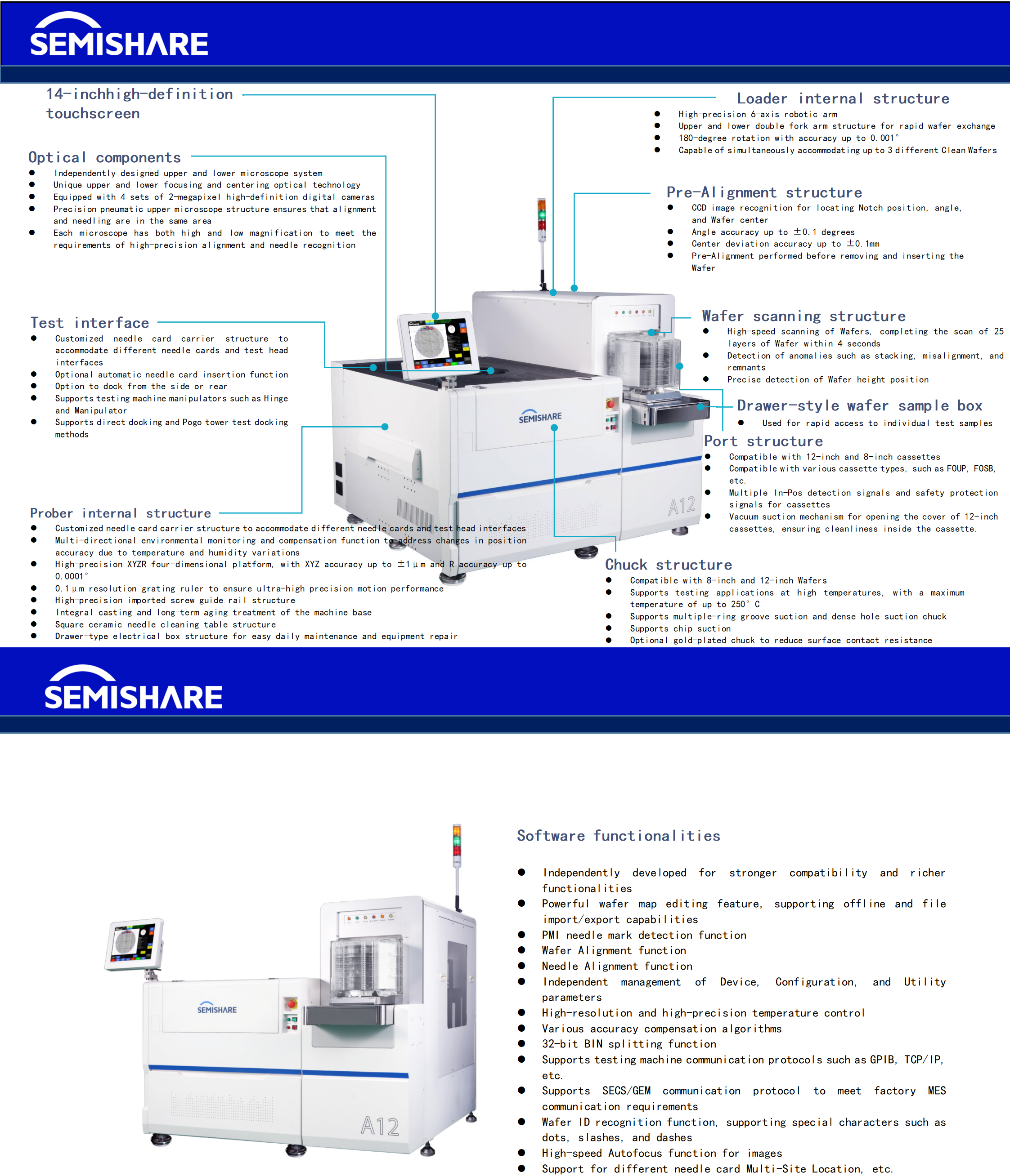
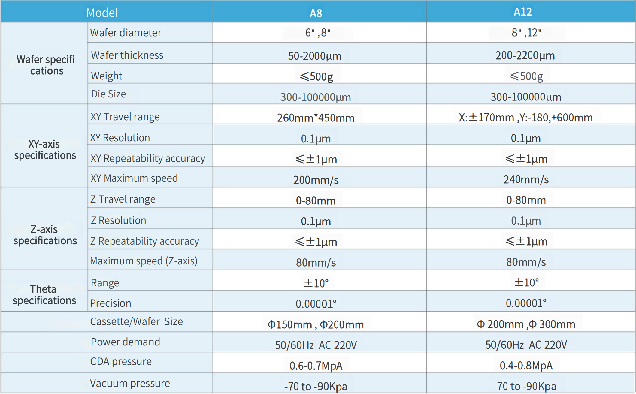
SEMISHARE's A Series: The Pinnacle of Automatic Probe Station Technology
The A Series Full Automatic Probe Station represents the culmination of SEMISHARE's years of research and development in semiconductor testing technology. This production-ready automatic high and low-temperature probe station boasts unparalleled test precision and speed, setting new standards in the industry.
Key features of the A Series include:
1. Automatic material handling for efficient wafer loading and unloading
2. Advanced wafer alignment and centering systems for precise positioning
3. Automatic die size testing and wafer ID identification
4. Versatile testing capabilities, including single-point and continuous testing modes
5. Rich, feature-packed test software for enhanced productivity and efficiency
Available in A8 and A12 models, the A Series caters to different production scales and requirements, offering:
- Micron-scale fully closed-loop motion control for ultimate precision
- High voltage and high current test applications
- Bernoulli arm support for stable wafer handling
- Compact design for efficient use of laboratory or production floor space
- 24/7 operational capability for maximum throughput
The A12 model, in particular, pushes the boundaries of what's possible in automatic probe station technology, featuring:
- Super-high test precision and speed for unmatched productivity
- Fully automated system operation ensuring fast, safe, and reliable testing
- Integrated control system for seamless instrument integration
- High-speed chuck system with movement speeds exceeding 300mm/s
- Advanced software automation and precise mechanical calibration
- Optional automatic wafer thickness measurement and ID reading capabilities
- Industry-leading internal anti-shock system for stable operation
The Future of Semiconductor Testing with SEMISHARE's Aotomatic Prober and Auto Prober Technologies
As the semiconductor industry continues to evolve, so too does the technology required to test these increasingly complex devices. SEMISHARE is committed to staying at the forefront of this evolution, continually refining and improving our aotomatic prober and auto prober technologies.
Looking ahead, we anticipate several key trends in semiconductor testing that our aotomatic prober and auto prober systems are well-positioned to address:
1. Increased Test Complexity: As devices become more sophisticated, the number and complexity of tests required will increase. Our aotomatic prober and auto prober systems are designed with the flexibility to adapt to these changing requirements.
2. Higher Frequencies: With the advent of 5G and beyond, testing at ever-higher frequencies will become crucial. SEMISHARE's aotomatic prober and auto prober technologies are being developed to handle these high-frequency testing needs.
3. Smaller Feature Sizes: As semiconductor devices continue to shrink, the precision required for testing increases. Our aotomatic prober and auto prober systems are constantly being refined to offer even greater accuracy at smaller scales.
4. Integration of Machine Learning: The future of semiconductor testing lies in intelligent systems that can learn and adapt. SEMISHARE is investing heavily in integrating machine learning capabilities into our aotomatic prober and auto prober technologies.
5. Enhanced Reliability Testing: With semiconductors being used in increasingly critical applications, reliability testing becomes paramount. Our aotomatic prober and auto prober systems are being enhanced to provide even more comprehensive reliability testing capabilities.
Conclusion: SEMISHARE's Commitment to Advancing Semiconductor Testing
In the rapidly evolving field of semiconductor manufacturing, the role of precise and reliable testing cannot be overstated. SEMISHARE's comprehensive range of automatic probe stations, including our advanced aotomatic prober, automatic probe station, and auto prober technologies, offers semiconductor manufacturers and researchers the tools they need to ensure the quality and performance of their devices.
Our commitment to innovation, precision, and customer service positions SEMISHARE as a trusted partner in the semiconductor industry. By continually pushing the boundaries of what's possible in semiconductor testing, we enable our clients to stay at the forefront of technological advancement, driving progress in fields ranging from consumer electronics to quantum computing.
Whether you're developing cutting-edge processors, high-performance memory devices, or next-generation sensors, SEMISHARE has the automatic probe station solutions you need to ensure the quality and reliability of your innovations. Visit https://www.semishareprober.com/ to explore how our advanced probe station technology can elevate your semiconductor testing capabilities and drive your success in this dynamic industry.