Wafer Probing Machine Tester with the X12 | SEMISHARE
The X12 semi-automatic wafer probing machine tester,a powerful wafer probing solution which can work 7*24 hours at -60℃ to 300 ℃ to meet customers' unique testing needs.
SEMISHARE: Revolutionizing Semiconductor Testing with Advanced Wafer Probing Solutions
In the ever-evolving landscape of semiconductor manufacturing, the demand for precise, efficient, and reliable testing solutions has never been greater. SEMISHARE stands at the forefront of this technological revolution, offering cutting-edge wafer probing, wafer prober tester, and wafer probing machine technologies that are reshaping the landscape of semiconductor testing. Our commitment to innovation is evident in our state-of-the-art solutions designed to meet the most stringent demands of modern semiconductor research and production.
Understanding Wafer Probing: The Foundation of Semiconductor Quality Assurance
What is wafer probing? At its core, wafer probing is a critical process in semiconductor manufacturing that involves electrically testing semiconductor wafers before they are diced into individual chips. This essential step ensures the functionality and performance of each device, playing a pivotal role in identifying defects and maintaining the highest standards of quality in semiconductor production.
SEMISHARE's wafer probing solutions take this concept to new heights, offering unparalleled precision and efficiency in semiconductor testing. Our advanced wafer probing technologies integrate cutting-edge automation with high-precision measurement capabilities, allowing for rapid and accurate testing of complex semiconductor devices.
The Evolution of Wafer Prober Testers
The wafer prober tester has come a long way since its inception. SEMISHARE's latest wafer prober tester models represent the pinnacle of this evolution, incorporating advanced features that significantly enhance testing capabilities:
1. Multi-Site Testing: Our wafer prober tester can simultaneously test multiple dies on a wafer, dramatically increasing throughput.
2. Adaptive Testing Algorithms: The wafer prober tester can adjust testing parameters in real-time based on initial results, optimizing the testing process for each unique device.
3. Integrated Data Analytics: Our wafer prober tester includes powerful analytics tools, providing in-depth insights into device performance and helping identify trends and potential issues early in the production process.
4. Advanced Probe Card Compatibility: SEMISHARE's wafer prober tester is designed to work with a wide range of probe card technologies, offering flexibility in testing approaches.
The Wafer Probe Test Process: A Symphony of Precision and Efficiency
The process of wafer probe test is a sophisticated dance of technology and precision. It begins with the careful mounting of the wafer onto a specialized probing station. SEMISHARE's wafer probing machine is engineered to handle this delicate process with utmost care, ensuring the wafer's integrity throughout the testing procedure.
Once mounted, the wafer prober tester aligns the probes with the wafer's test pads using advanced optical recognition and alignment systems. This crucial step is where the precision of SEMISHARE's technology truly shines, ensuring accurate contact even with the smallest of test pads.
With alignment complete, the wafer probing machine conducts a series of electrical measurements as defined by the user. These tests can range from basic parametric measurements to complex functional assessments, all executed with the high precision and speed that SEMISHARE's technology is known for.
Advancements in Wafer Probing Machine Technology
SEMISHARE's wafer probing machine technology has seen significant advancements in recent years:
1. Enhanced Precision: Our latest wafer probing machine models offer positioning accuracy down to the sub-micron level, crucial for testing the latest generation of semiconductor devices.
2. Improved Environmental Controls: The wafer probing machine now incorporates advanced temperature and humidity control systems, ensuring consistent test conditions across long test runs.
3. Increased Automation: SEMISHARE's wafer probing machine features enhanced automation capabilities, reducing the need for manual intervention and minimizing the risk of human error.
4. Advanced Imaging Systems: Our wafer probing machine includes high-resolution imaging systems for real-time observation and analysis of the probing process.
5. Integrated Fault Detection: The wafer probing machine now includes sophisticated fault detection algorithms, identifying potential issues before they can impact test results.
The Role of Probes in Semiconductor Testing
A probe in semiconductor testing is more than just a simple contact point. It's a sophisticated tool designed to transmit electrical signals to and from the device under test with minimal interference. SEMISHARE's probes are engineered for optimal performance, ensuring reliable contact and accurate measurements across a wide range of testing scenarios.
Our probe technology stands out for its:
1. High-precision tip geometry for accurate contact
2. Advanced materials for durability and consistent electrical properties
3. Customizable configurations to meet specific testing requirements
4. Compatibility with a wide range of test parameters and conditions
The Probing Process: A Delicate Balance of Technology and Technique
The probing process is a meticulous procedure that requires both advanced technology and skilled execution. SEMISHARE's wafer probing solutions are designed to streamline this process, offering:
1. Automated alignment systems for precise probe positioning
2. Real-time force feedback to ensure optimal contact pressure
3. Multi-site probing capabilities for increased throughput
4. Advanced imaging systems for accurate pad recognition and probe placement
What Does a Wafer Prober Do?
A wafer prober is a sophisticated machine designed to perform detailed electrical measurements on semiconductor wafers. SEMISHARE's wafer prober goes beyond basic functionality, offering:
1. High-speed testing capabilities for increased productivity
2. Wide temperature range testing for comprehensive device characterization
3. Integration with various measurement instruments for versatile testing scenarios
4. Advanced data analysis tools for real-time performance evaluation
The Wafer Tester: A Critical Tool in Semiconductor Manufacturing
A wafer tester is an essential device in the semiconductor manufacturing process, used to evaluate the electrical characteristics of semiconductor wafers. SEMISHARE's wafer tester technology offers:
1. High-precision measurement capabilities across a wide range of parameters
2. Flexible test program development for customized testing requirements
3. Integration with automated handling systems for high-volume testing
4. Comprehensive data logging and analysis for quality control and process improvement
Understanding the Prober: The Heart of Wafer Testing
A prober is the core component of any wafer testing system. It's responsible for making contact with the wafer's test pads and facilitating the electrical tests. SEMISHARE's probers are designed for:
1. High-precision positioning for accurate contact
2. Stable operation for consistent measurements
3. Compatibility with various probe card technologies
4. Easy maintenance and calibration for long-term reliability
The Wafer Probing Machine: A Marvel of Modern Engineering
SEMISHARE's wafer probing machine represents the pinnacle of semiconductor testing technology. This advanced system integrates multiple technologies to provide a comprehensive testing solution:
1. High-speed wafer handling for improved throughput
2. Precision probe alignment for accurate measurements
3. Advanced environmental controls for testing across a wide temperature range
4. Integrated data management systems for comprehensive test reporting
How Are Wafers Tested? The SEMISHARE Approach
SEMISHARE's approach to wafer testing combines advanced technology with efficient processes:
1. Automated wafer loading and alignment using our state-of-the-art wafer probing machine
2. Precision probe contact using advanced force control systems integrated into our wafer prober tester
3. Comprehensive electrical testing using our wafer probing machine's integrated measurement instruments
4. Real-time data analysis and reporting for immediate quality assessment, a key feature of our wafer prober tester
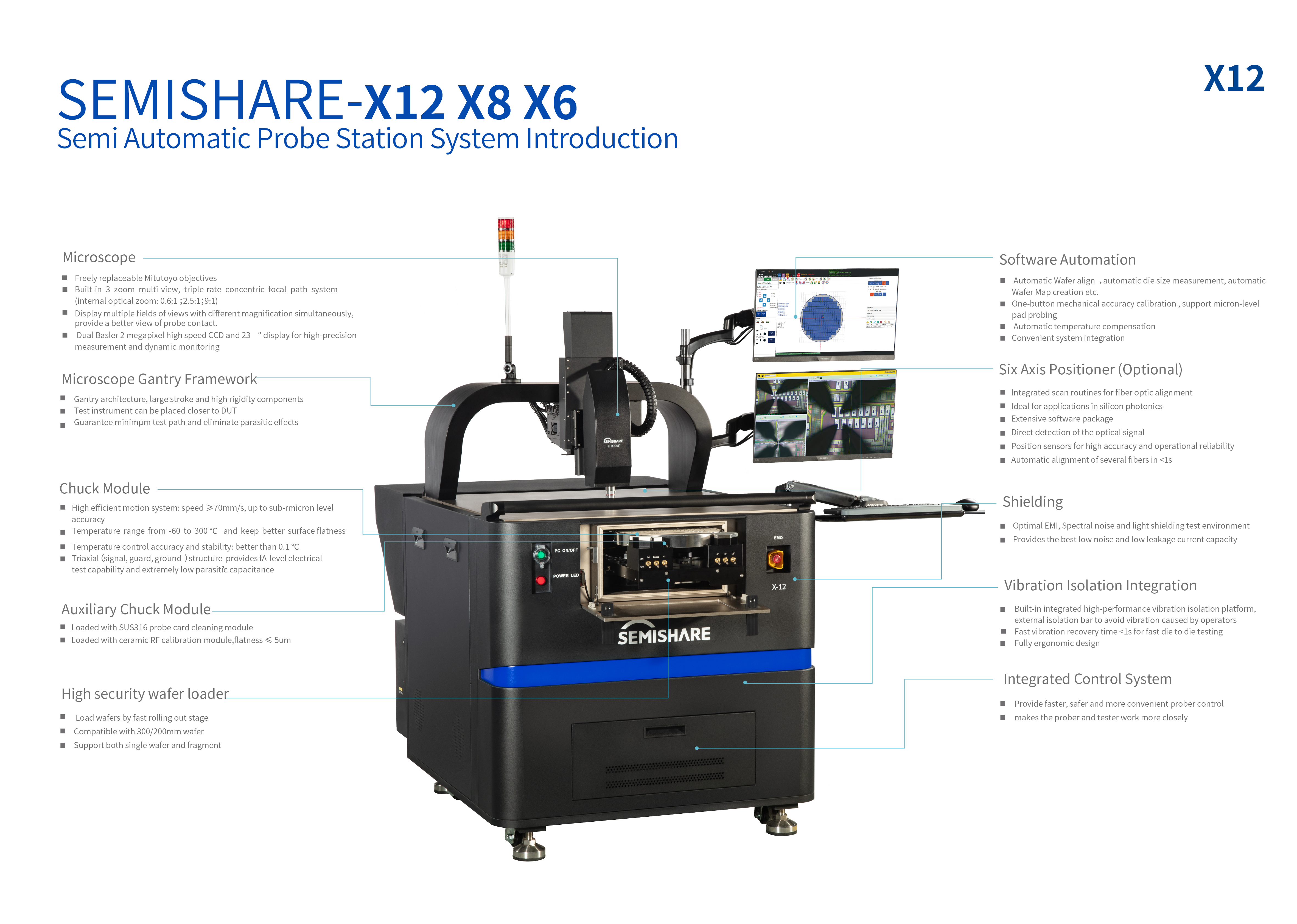
SEMISHARE's X Series Semi-Automatic Probe Station: Setting New Standards in Wafer Testing
The X Series Semi-Automatic Probe Station represents the culmination of SEMISHARE's expertise in wafer probing technology. This integrated and highly efficient wafer probing machine is specialized in testing the performance of various advanced chips, offering:
1. Versatile functionality, including electric, optical, and microwave testing capabilities
2. Industry-leading temperature range (-60°C to 300°C) for comprehensive device characterization
3. Superior test accuracy for reliable results
4. Customizable configurations to meet specific testing requirements
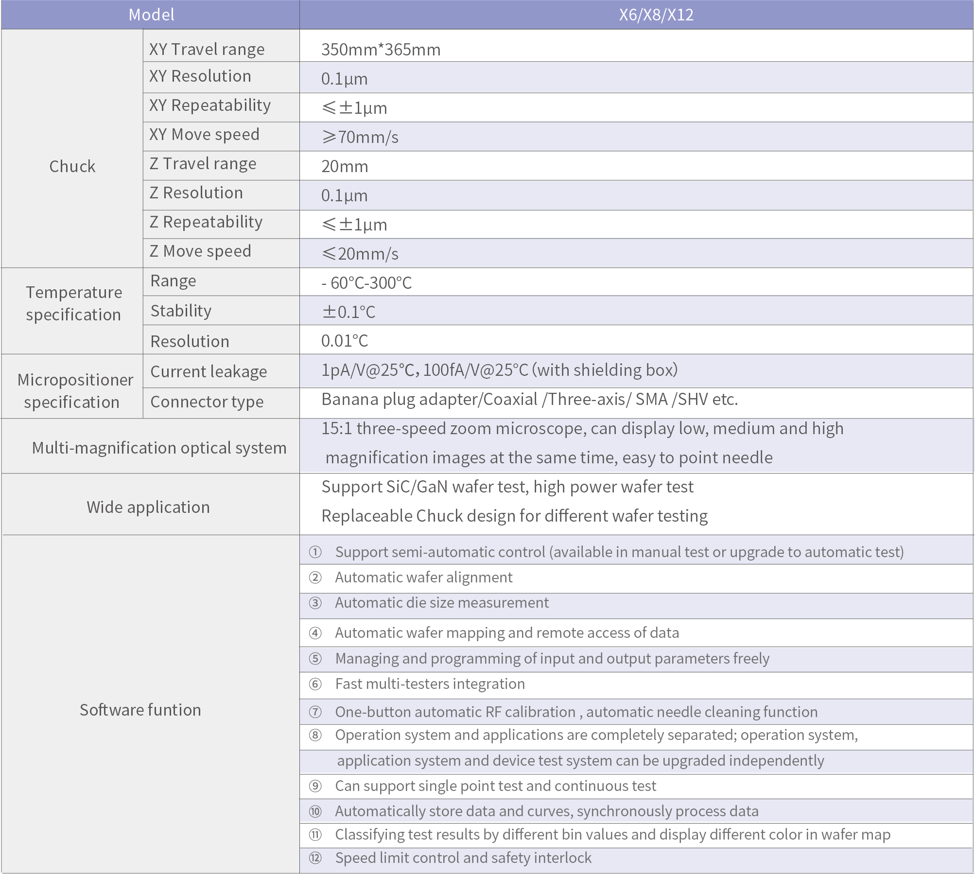
Technical Highlights of SEMISHARE's Wafer Probing Solutions
1. Efficient CHUCK System: Our wafer probing systems, including our advanced wafer prober tester, increase test efficiency by more than 40%, with a running speed exceeding 70mm/s and motion precision of 1 micrometer.
2. Advanced Imaging Technology: We incorporate industry-leading three zoom microscope views with high-speed CCD and high-precision cameras for precise positioning and high-definition imaging in our wafer probing machine.
3. Innovative CHUCK Module Design: Our unique Chuck XY axis design ensures higher motion precision and stability in our wafer prober tester, with a larger rotation angle range for more flexible and convenient operation.
4. O-type Needle Seat Platform: Our wafer probing machine design allows for the placement of up to 12 needle seats, increasing testing efficiency by 50%.
5. Proprietary Airfilm Shock Absorption System: This system ensures stable operation and precise control of the platform's moving parts in our wafer prober tester, even at high speeds.
6. Advanced Anti-interference Shielding System: Our closed shielding cavity reduces system noise and blocks interference effectively, providing a superior test environment for weak electric signal testing in our wafer probing machine.
7. Software Integration: SEMISHARE's wafer prober tester and wafer probing machine come with advanced software that allows for easier control and data analysis, streamlining the testing process.
8. Customization Options: Our wafer probing machine and wafer prober tester can be customized to meet specific testing needs, ensuring that our clients have the exact tools they need for their unique applications.
Conclusion: SEMISHARE's Commitment to Advancing Semiconductor Testing
In the dynamic field of semiconductor technology, the ability to perform precise and reliable wafer probing is becoming increasingly crucial. SEMISHARE's comprehensive range of wafer probing, wafer prober tester, and wafer probing machine solutions offers semiconductor manufacturers and researchers the tools they need to push the boundaries of device performance and reliability.
Our commitment to innovation, precision, and customer support positions SEMISHARE as a trusted partner in the semiconductor industry. By continually advancing our wafer probing technologies, including our state-of-the-art wafer prober tester and wafer probing machine, we enable our clients to stay at the forefront of semiconductor development, driving progress in fields ranging from consumer electronics to advanced computing systems.
Whether you're developing cutting-edge processors, high-performance memory devices, or next-generation sensors, SEMISHARE has the wafer probing solutions you need to ensure the quality and reliability of your innovations. Our wafer prober tester and wafer probing machine are designed to meet the most demanding testing requirements, providing the accuracy and efficiency needed in today's fast-paced semiconductor industry.
Visit https://www.semishareprober.com/ to discover how our advanced wafer testing technologies, including our cutting-edge wafer prober tester and wafer probing machine, can elevate your semiconductor research and production capabilities, propelling your success in this dynamic and challenging industry. With SEMISHARE's wafer probing solutions, you're not just testing semiconductors – you're shaping the future of technology.