Advanced Manual Probers Solutions - SEMISHARE Prober
Embark on a journey of semiconductor testing finesse with our manual prober collection. Dive into SEMISHARE Prober's unique manual prober solutions for precision.
SEMISHARE: Pioneering Manual Prober Technology in Semiconductor Testing
In the intricate world of semiconductor testing, precision and reliability are paramount. SEMISHARE's H Series Integrated Manual Probe Station stands at the forefront of manual prober technology, offering unparalleled performance for a wide range of semiconductor testing applications. This article delves into the nuances of manual probers, their critical role in semiconductor development, and the innovative features that set SEMISHARE's technology apart.
Understanding the Manual Prober
A manual prober, the cornerstone of semiconductor testing in many research and development settings, is a sophisticated device designed for hands-on electrical testing of semiconductor wafers and chips. Unlike automated systems, a manual prober allows for direct user control, making it invaluable for detailed analysis and specialized testing scenarios.
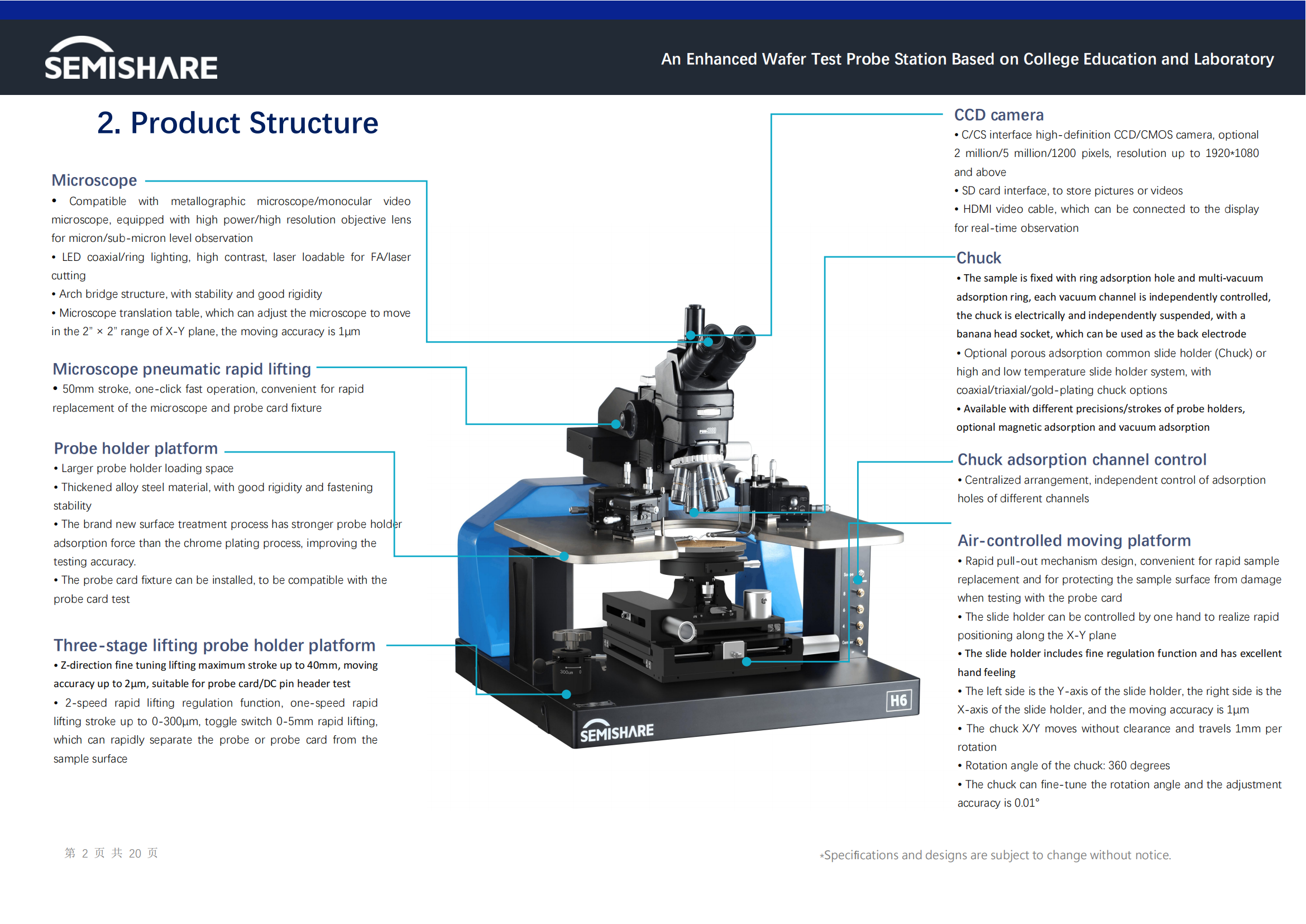
Key Components of a Manual Prober:
1. Probe Platen: The platform where probe positioners are mounted.
2. Chuck: A specialized stage that holds the wafer or device under test.
3. Microscope: For visual inspection and precise probe placement.
4. Probe Positioners: Mechanical arms for precise probe movement.
5. Vibration Isolation System: To minimize external disturbances.
SEMISHARE's H Series manual prober integrates these components with advanced technologies, creating a system that excels in precision, stability, and user-friendliness.
The Evolution of Manual Prober Technology
Manual probers have come a long way since their inception. Early models were basic mechanical devices with limited precision. Today's manual probers, like SEMISHARE's H Series, incorporate advanced materials, precision engineering, and sophisticated control systems.
Key advancements in manual prober technology include:
1. Improved Positioning Accuracy: From millimeter to sub-micron precision.
2. Enhanced Vibration Isolation: Using active and passive damping systems.
3. Integration of Digital Imaging: For real-time visual feedback.
4. Advanced Chuck Technologies: Including thermal control and air-bearing systems.
5. Software Integration: For data collection, analysis, and process automation.
SEMISHARE's Innovations in Manual Prober Design
Chuck Air Bearing Move Technology
This groundbreaking feature in SEMISHARE's manual prober revolutionizes wafer handling:
1. Frictionless Movement: Allows for smooth, precise wafer positioning.
2. Reduced Contamination: Minimizes particle generation during movement.
3. Enhanced Throughput: Enables faster repositioning between test points.
4. Improved Accuracy: Eliminates stick-slip effects common in mechanical systems.
The air bearing system uses a thin film of pressurized air to float the chuck, reducing friction to near-zero levels. This not only improves positioning accuracy but also extends the life of the chuck mechanism.
Large Handle Differential Head Drive
This ergonomic innovation significantly enhances user experience and precision:
1. Intuitive Control: Large handles provide better tactile feedback.
2. Fine Adjustment: Differential mechanism allows for micrometer-level adjustments.
3. Reduced Operator Fatigue: Ergonomic design for extended use.
4. Increased Stability: Minimizes unintended movements during adjustment.
The differential head drive combines coarse and fine adjustment capabilities, allowing operators to make precise movements with ease. This is particularly crucial when working with dense semiconductor layouts.
Microscope Air-Controlled Lifting Control
This feature enhances both functionality and safety:
1. Smooth Vertical Movement: Precision air control for focus adjustments.
2. Collision Prevention: Automated safeguards to prevent accidental contact.
3. Extended Working Distance: Facilitates easier wafer and probe manipulation.
4. Rapid Objective Changes: Streamlines workflow for different magnification needs.
The air-controlled system provides a level of control and safety not possible with manual lifting mechanisms, ensuring the delicate balance between close observation and wafer protection.
Three-Stage Lifting Needle Base Platform
This advanced system offers unparalleled flexibility in probe positioning:
1. Rapid Height Adjustment: Quick transitions between test, separation, and loading positions.
2. Micrometer-Level Precision: Fine control for exact probe placement.
3. Consistent Repeatability: Ensures reliable results across multiple tests.
4. Enhanced Safety Features: Incorporates locks to prevent accidental movements.
The three-stage system allows for both rapid gross adjustments and ultra-fine positioning, catering to a wide range of testing scenarios.
Applications of Manual Probers in Modern Semiconductor Testing
Manual probers find applications across various sectors of the semiconductor industry:
1. Research and Development
- New Material Characterization: Testing electrical properties of novel semiconductor materials.
- Device Prototyping: Evaluating performance of experimental chip designs.
- Failure Analysis: Identifying and analyzing defects in semiconductor devices.
2. Low-Volume Production
- Custom IC Testing: For specialized or small-batch integrated circuits.
- MEMS Device Evaluation: Testing micro-electromechanical systems.
- Photonic Device Characterization: Analyzing optoelectronic components.
3. Educational Institutions
- Hands-on Training: Teaching semiconductor testing principles to students.
- Academic Research: Supporting cutting-edge studies in microelectronics.
4. Quality Control
- Spot-Checking: Verifying the quality of production batches.
- Process Validation: Ensuring manufacturing processes meet specifications.
5. Specialized Testing Environments
- High/Low Temperature Testing: Evaluating device performance under extreme conditions.
- High-Frequency Testing: Characterizing RF and microwave devices.
- High-Power Device Testing: Assessing performance of power semiconductors.
SEMISHARE's manual prober excels in these applications, offering the flexibility and precision needed for diverse testing requirements.
The Role of Software in Manual Prober Operations
While the physical components of a manual prober are crucial, the software interface plays an equally important role:
1. Test Pattern Generation: Creating custom test sequences for specific devices.
2. Data Acquisition and Analysis: Collecting and processing test results in real-time.
3. Probe Positioning Control: Assisting in precise probe placement and movement.
4. Environmental Monitoring: Tracking and controlling test conditions.
5. Integration with External Instruments: Coordinating with other test equipment.
SEMISHARE's prober software is designed for intuitive operation while offering advanced capabilities for data management and analysis.
As semiconductor technology continues to advance, manual probers are evolving to meet new challenges:
1. Increased Automation: Integration of automated features for repetitive tasks.
2. Enhanced Resolution: Pushing the boundaries of probe positioning accuracy.
3. Advanced Materials: Incorporating new materials for improved performance and durability.
4. IoT Integration: Connecting probers to the broader manufacturing ecosystem.
5. AI-Assisted Testing: Implementing machine learning for test optimization and fault detection.
SEMISHARE is at the forefront of these developments, continuously refining its manual prober technology to meet the evolving needs of the semiconductor industry.
In the rapidly evolving field of semiconductor technology, the role of precise and reliable testing equipment is more critical than ever. SEMISHARE's H Series Integrated Manual Probe Station represents the pinnacle of manual prober technology, offering unparalleled precision, versatility, and user-friendliness.
From its innovative Chuck Air Bearing Move Technology to its ergonomic Large Handle Differential Head Drive, every aspect of SEMISHARE's manual prober is designed to enhance the testing process. Whether used in cutting-edge research laboratories, educational institutions, or specialized production environments, this manual prober provides the tools necessary to push the boundaries of semiconductor technology.
As the semiconductor industry continues to advance, with devices becoming smaller, more complex, and more powerful, the need for sophisticated testing equipment grows. SEMISHARE's commitment to innovation ensures that its manual prober technology evolves in tandem with these industry developments, providing researchers and engineers with the tools they need to shape the future of electronics.
For those seeking to elevate their semiconductor testing capabilities, SEMISHARE's manual prober offers a compelling solution. Its combination of precision, flexibility, and advanced features makes it an indispensable tool in the quest for semiconductor innovation and quality assurance.
To learn more about how SEMISHARE's manual prober can enhance your semiconductor testing processes, visit our website at https://www.semishareprober.com/. Discover the difference that precision, reliability, and innovation can make in your semiconductor testing endeavors.