Test Solution
Power devices are a general term for electronic components and devices which are the core of energy conversion and circuit control in electronic devices. They use the unidirectional conductivity of semiconductors to change the functions of voltage, frequency, phase, and DC/AC conversion in electronic devices. High-power devices generally refer to electronic components with voltage levels above 1200V, current levels above 300A, and relatively high output power. Typical high-power devices include high-power diodes, thyristor SCR, bipolar power transistor IGBT, power transistor GTR, IGCT, GTO, ETO, SIT, etc. Power semiconductors are widely used in industries such as new energy (wind power, photovoltaics, electric vehicles), consumer electronics, smart grids, and rail transit. IGBT and MOSFET, as the main power electronic devices, are widely used in computers, communication, etc. The radio frequency semiconductor with gallium nitride (GaN) as the core supports the construction of 5G base stations and industrial Internet systems; Power semiconductors with silicon carbide (SiC) and IGBT as their core support the construction of new energy vehicles, charging stations, base station/data centre power supplies, ultra-high voltage, and rail transit systems.
Driven by the steady growth of the market space for power semiconductors, the performance requirements for semiconductors are constantly improving. Ensuring that the selected high-speed power devices can operate stably and reliably in high temperature, intense radiation, and high-power environments poses significant testing challenges for design engineers. We need to understand the dynamic characteristics of power devices:
The electrical measurement of high-power separated components (such as power transistors, power diodes, gate fluids, etc., with vertical/horizontal directional components) or high-power amplifiers belongs to high-power component testing. Measure with pulses or direct current of 500 V (high voltage) or above and 1 A (high current) or above. The wafer characteristics of high-power components face the following challenges in application: contact resistance from the wafer carrier to the back of the wafer/burning and damage of high current component metal cushion layer/low leakage current measurement under high voltage and various temperature conditions/high voltage arc/thin wafer processing/safe testing environment.
>SEMISHARE X Series Semi-Automatic Wafer ProberLearn More
>SEMISHARE High-Temperature High-Pressure Three-Axis ChuckLearn More
>SEMISHARE SS-125-m Submicron Circuit/RF Test Probe StationLearn More
**Semiconductor sample:GaN
Needle holder movement accuracy is 0.6um, chuck leakage current is ≤100fA, chuck and microscope XYZ movement accuracy is 0.1um, withstand voltage of 3K-10KV, and withstand temperature of 200℃.
1. Manual loading: The software controls the chuck removal, manually places the wafer on the chuck, opens the adsorption switch to adsorb the wafer, and moves the chuck to the cavity, then controls the chuck to return to its original position.
2. The software controls the motor to move the chuck and the microscope up and down until the surface of the wafer can be preliminarily seen. The automatic focusing function can be used to focus on the surface quickly.
3. Use the automatic straightening function to adjust the wafer water rotation until level.
4. Use high-Voltage fixtures and three-axis probes to tie onto the corresponding PAD accurately.PAD
5. Check the contact between the probe andPADPAD and the connection of the tester. Drip fluorine oil onto the needle and place it under high Voltage for ignition before applying an electrical signal for testing.
1. The chuck and microscope are controlled by software to move the motor, with a movement accuracy of 0.1um.
2. Equipped with a built-in3 zoomthree zoom multi-field of view, triple magnification confocal optical path system, displaying multiple fields of view simultaneously, providing an extremely convenient needle-pointing experience.
3. High-voltage chucks, high-voltage fixtures, and shunt probes can withstand high voltage and current conditions during power testing.
4. Equipped with an integrated high-performance vibration isolation platform and an external isolation barrier, it avoids vibrations caused by operators. The fast vibration recovery time is less than <1 second,providing a high-stability environment for testing.

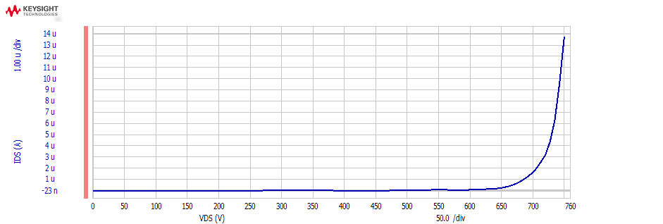
Horizontal device testing (vertical devices can be tested using chuck back electrodes)